
Optimizing board level embedded hardware with shared (interleave) memory, containing processors and video devices, using sync and phase lock methods
Modern day performance improvements are available for the ARM, PIC, open source RISC-V, and 65xx families of CPU/MPU/SoC, by optimizing the interleaving of DRAM memory bus cycles, and improving synchronizing timing, resulting in 10 to 15 percent more memory bus cycle availability and video performance. Improvements of process synchronization and phase lock can be done at both the IC-design level and the PC-board design/firmware level.
Legacy examples of re-usable 1980’s Atari and Commodore of video engines (VDU/GPU) hardware and existing ARM MPU/SoC Gated-Clocks software controlled hardware are listed. These synchronous methodologies can implement both at board level designs and on-chip design enhancements for fully or partially synchronous systems, allowing slower bus clocks, cost savings, power savings, and improved real time deterministic performance.
- Abstract
Electronics SoC board and chip designers can benefit from periodically turning-off ARM/PIC LCD/OLED Raster-data-stream of the processing/display raster. Designers need to minimize cost of build, cost of development, time-to-market, and reduce wattage consumption. Synchronous methods for Systems-On-A-Chip (SOC) are being reviewed especially for modern products that often have multiple processors and displays.
How to turn-off ARM/PIC LCD RASTER data stream, and guarantee no display artifacts issues? In general, this is done by both controlling when to turn off the raster scan, and assuring the raster scan gets turned back on, at the correct time. The more synchronous like control of display rasters, for power savings, and memory bus cycle share budgets, can be both in hardware like the early 8 bit PC and game machines or with Gated-Clock circuits often overlooked in ARM-SOC Commercial off the Shelf (COTS) IC’s that have VDU/GPU engines.
In the 1980’s popular personal computers had main CPU memory bus speeds usually under 2 MHz. The challenge with this early technology was IC design limitations, where every bus cycle was counted and carefully planned for by the hardware chip designers and often also by application programmers. In modern times SoC-CPU bus speeds and DRAM are so fast (more MIPS capable than the board designer sometimes needs) that most board designers are unaware of the complex bus management of asynchronous processes that go on in the SoC chip. This is where the CPU, VDU/GPU and DRAM refresh compete for memory cycles across multiple asynchronous clock speed domains.
Because of interleaved memory (where multiple processes share one memory bus) bus cycle overload, careful control of video display frame phase locking can be the zero cost solution. No additional dedicated display memory is needed, on low cost systems, if display video memory reads do not interfere with other processors sharing the bus, competing for memory reads and writes. The video frames phase lock improvement apply to both display and camera input processes.
Video frame timing phase locking, and/or horizontal scan line timing phase locking, can improve the memory bus sharing behavior, balancing the memory accesses for display-reads and general purpose read-writes.
Not just 65XX, ARM and PIC small processors in small consumer products that have eaten away at the X86 market like termites eating a wooden battleship, but even Intel and Microsoft small laptops and notepads are returning to lower cost interleaved memory architecture design philosophy.
Similar to 1980’s 8-bit PC’s, older Apple-II, Atari, C64, are rolling-stock-vehicles like the VW Beetle, and Jeep-XJ which are lean innovative products. Some of these example product lists are fast implemented designs that have noteworthy cost and reliability ramifications for the end users. Profitable, reliable, and high-value designs for the end-users, and systems engineers, are all about design trade-offs and design-margins.
Overall, the reason for synchronizing processors and video functions is to get more usable MIPS (millions of instructions per second) out of the hardware, resulting in improved deterministic real time behavior, in both computing and video display images. It is best used for mass produced products. This can include greater attention to details of PC-board design and firmware, and/or at the IC-design that is better optimized to take full advantage of the improved hardware.
- Asynchronous Interleave Memory Design Architectures have Metastability Issues
It is for the same reason DRAM bits have replaced SRAM bits, by numbers of bits in chips, worldwide in all IC production, and by possibly over 99%.
Interleaved DRAM memory design architecture is better in the vast majority of low-priced products with processors and displays, concerning the typical and appropriate designer’s requirements list:
Processing/display board design goals:
- reduce cost of build,
- reduce cost of development,
- reduce time-to-market,
- reduce wattage consumption,
- reduce size,
- improve product build life, with an easier supply chain, smaller parts list,
- remove clock timing issues of metastability, remove busiest flops in the design,
- improve temporal (timing) repetitive alignment of computing and display results.
Whole OEM product, boxed retail to Line Replace-able Units (LRU) in a system (such as an automobile): When any card, or subsystem needs more cost, more space, more power (and makes more heat); every sub-system add-on can result in increasingly deleterious performance and/or behavior of the system.
Whole OEM product/LRU design goals:
- reduce space, heat, power,
- reduce cost of development,
- reduce time to market,
- improve end-product performance for customer experience.
For a tabletop DVD player, higher power consumption makes the system cost more. But the heat and wattage issues may be unnoticed, that burden being moved to the customer’s hidden costs.
However, for a car-radio-MP3-player, if it comes in over-size, overweight, over-wattage, over-cost; the results can make the larger design team re-design the dashboard, or retrofit an older less desirable radio-player. If multiple subsystems increase wattage, the team may have to increase air-conditioning BTU ability and up-scale the alternator and main 12V battery.
Another vehicle example is the 2014 Prius total weight reaching 3050 lbs, and typical vehicle features, such as ride quality or repair-ability, had to be dropped, so that the small, but very heavy, car would not burst its small tires. Again the “lean” vehicle example, is the Jeep-XJ-SUV, 4-Door, 4WD weighed the same 3050 lbs, with 30 inch outer diameter tires. The experimental Prius probably should not have been mass produced; other factors including income-tax rebates prevailed.
Interleaved memory designs are all about cost reduction. That affects a number of variables of whether an electric processor/display board is a market winner. It also has carry over effects on the larger systems, from boxed retail DVD players to Line Replaceable Units (LRU) in a system (such as an automobile).
By having a fully synchronized System on a chip (SOC) design, of computing, video, and sound; then only a few slower ports need to use localized serialized sets of D-flip-flops that are in effect small FIFO’s. These cross-clock-boundary serialized sets of D-flip-flops, when between main processing and video, can be as much as 80% of R/W transfers on the main memory bus. The cross-clock-boundary serialized sets of D-flip-flops also further consume watts, and slow processes need faster local clocks or additional clock phases.
2.1 65xx DRAM Refresh and Cross-Domain Clock Speeds
Improved write-up white papers have appeared on the internet that describe many details, of the Atari and Commodore interleave memory designs, to include a C64 meta-stable RAS-CAS DRAM refresh timing design flaw. This C64 flaw is not from the synchronous DRAM-R/W’s of the CPU and the competing Vic-II video chip DRAM-Reads. Rather it is that DRAM refresh can start sometimes at a fixed time in a horizontal blank, when the last CPU instruction may not yet be completed, if it was an uncommonly many clock-cycle count command.
What could be the most important thing lacking in the old classic 6502 and 6510 CPU chip design through the mid-1980’s was that the 65XX CPU chip came with no proven built-in, or companion, chip for DRAM management.
The 65XX DRAM manager function was left to the board designer. Today, in the decade starting in 2020, this is rather an easy fix of adding some premade functions (comprising gates and flops) at a fabless design house. This 65XX improvement is adding standard DRAM RAS-CAS refresh, along with a bus cross-clock-domain manager. (The cross-clock-domain manager handles the task of different clock speeds on buses that periodically connect at random times, with almost no data errors.)
These DRAM management and metastability of cross-domain bus-speed issues, seem to get little discussion in the processor design magazines and blogs. It is sort of like how architectural home design magazines don’t talk much about dirty issues of plumbing and sewer design.
Overall, the Atari-400/800 and C64 don’t have cross-domain bus-speed issues, due to the overall synchronous CPU/display-video designs. These two brands of 65XX CPU personal computers do still have some peripheral I/O chips that connect port data values to the main memory bus. But the external peripheral ports speeds are so slow as not to be much of a cross-domain bus clock speed issue.
Virtually all ARM CPUs today that connect to DRAM have a built in DRAM manager. The ARMs also come with built-in cross-domain bus handling. The board designers usually have no knowledge of these issues that have been taken care of in the ARM and PIC. ARM CPU chip designs have been no longer free for quite some time, but 65XX variants are shaping up to be fully open source.
https://webee.technion.ac.il/~ran/papers/Metastability%20and%20Synchronizers.posted.pdf
“Metastability events are common in digital circuits, and synchronizers are a must to protect us from their fatal effects. ….. Now, with multiple clock domains on the same chip, synchronizers are required when on-chip data across the clock domain boundaries.”
https://electronics.stackexchange.com/questions/14816/what-is-metastability
user3624 “The best way to deal with metastability is to make all of your logic synchronous, and not violate any of your setup and hold times. This is, of course, difficult to impossible for circuits of any complexity. So what we do is try to limit the places where metastability could be an issue and then deal with those places.
The normal method would be to “double-clock” the data. Meaning, have two D Flip-Flops in series with the output of the first feeding the input of the second”
IBM, following Apple, Atari, Commodore and others in the 1980’s PC market with the 8086/286 family processors, was worried of DRAM errors for main computing memory to the degree that a costly 9th bit was added for parity checking memory. The issues were similar to Commodore’s issue of metastability during RAS-CAS DRAM Refresh and crossing clock boundaries from main memory to the video card memory raster.
https://www.ardent-tool.com/FAQ/60/ps2faq.html
“IBM P/N 30F5360 / FRU 74X8637, which is a 1MB x 9 bit (Parity) 120ns module”
https://pdfcoffee.com/the-80×86-ibm-pc-and-compatible-computers-4th-editionpdf-pdf-free.html
“DATA INTEGRITY IN RAM AND ROM Checksum byte 284 Checksum program 286 Use of parity bit”
2.2 Intel, MS-HW, Atari, Apple, and Commodore Interleave Hardware Products
Intel has a more recent history of returning back to interleave memory design, where both the video raster and general computing memory are a single, synchronized, time-sliced shared address/data bus. Microsoft also, is recently producing ARM based interleave ultra-low cost mini laptop/pad PC’s.
https://www.intel.com/content/www/us/en/support/articles/000005657/boards-and-kits.html
Conversely, most higher-end priced x86 laptops and desktop PC’s have a dedicated separate video raster chip with dedicated video raster memory. Interleave memory architecture in personal computing is chip-set products that combine computation and display graphics rasters. It is a logical cost saving. This memory sharing method was made popular by the Atari-800-family Commodore-V64 and Apple-II on their history changing 8-system personal computer systems.
Articles have quoted Intel Inc. as saying, some few years past, that they would not produce a small ARM (typically with asynchronous display raster circuits built in) variant chip; thus embarrassingly pay license fees to ARM inc, that has interleave architecture, until hell-freezes over. A short span of years later, articles came out that “hell” had indeed frozen over.
In the latter part of the 2000’s decade, Intel actually went further into design and production of X86 low cost variant processors/companion chips that used interleaved memory design.
Earlier yet, in the 1970’s Apple-II, Atari 800, C-64 codified the interleave design philosophy as a core principle of the viability of the personal computers in the retail consumer market. These three early PC history makers did not just bring a new design method to computing; they were all three profitable, at least part or most of their corporate lives.
Management issues eventually took all three down. Apple re-emerged due to Bill Gates/Microsoft funding to stave off more monopoly lawsuits. Atari and Commodore managers and engineers simply could put their rivalry behind them and basically price warred each other out of business.
Apple Inc. came back with its “sexy” (Steve Jobs’ description) colorfully packaged “Mac” 68000 processor based computers, in the Microsoft/Intel style of bigger is always better. However, Apple’s ARM based cell-phone products, using interleaved DRAM design, again changed history, and all new levels of profitability were achieved.
But looking back in computer evolution to the 1970’s and 80’s, this interleave design method was done exceptionally well in most cases, and it was done with the slow chips of its era. Their names of Apple, Atari and Commodore stand out. All three were determined cost reducers and innovators.
https://en.wikipedia.org/wiki/Talk:MOS_Technology_6502/Archives/2011
6502 discussions have a new source of information as one of the designers is featured in an IEEE article. The 6502 Zero-Page processor function provided a very clever improvement for low cost computers and gaming products. A small sub-program, that is typically a smaller portion of a main-program, with its corresponding small block of data, staying under 256 bytes total; could run remarkably fast.
https://spectrum.ieee.org/amp/q-a-with-co-creator-of-the-6502-processor-2655032060
(Q&A With Co-Creator of the 6502 Processor Bill Mensch (BM) on the microprocessor that powered the Atari 2600 and Commodore 64)
“ (BM) Rod Orgill and I had completed the designs of a few microprocessors before the 6501/6502. In other words, Rod and I already knew what was successful in an instruction set. And lower cost was key. So we looked at what instructions we really needed. And we figured out how to have addressable registers by using zero page [the first 256 bytes in RAM]. So you can have one byte for the op code and one byte for the address, and [the code is compact and fast].
There are limitations, but compared to other processors, zero page was a big deal”…………….…” So when they (BM’s old co-workers at MOS-6502 project) had success with the ARM, I was cheering them on”
As noted in section “65xx DRAM Refresh and Cross-Domain Clock Speeds”, the popular ARM’s, RISC-V and PIC of modern times, have DRAM refresh function built-in. And with the high clocks speeds, has led to vast use of Commercial Off the Shelf (COTS) asynchronous MPU-SoC chip designs, where a FIFO pixel buffer for video raster, provided by the ARM, RISC-V, PIC MCU-SoC chip designer, output handles for the board design, these complex timing and buffering issues in an asynchronous system.
The famous designs of the early 1980’s Apple brand personal computers, using 6502 CPU chips, introduced the first very product successful use of one single DRAM bank (one address and memory bus) for general computing and video. The DRAM industry uses the Field Effect Transistor (FET) and capacitor to make a bit-cell, with a charge-leak time-contact, that suits reliable video memory function. Industry FET-DRAM’s design targets, of holding a reliable bit (capacitive charge) value, for about 64 msec, that is well beyond a 16 msec 60 Hz display screen or CRT-TV Set vertical blank rate. (a period where video needs no pixel data stream)
The DRAM of the 1980’s then, and now, is suitable for use in systems that can tolerate a wait state, while periodically the memory 1-bit cell can be reached. But this is the case only if the DRAM refresh is accounted for..
https://history-computer.com/Library/pat3387286ofDRAMmemory.pdf
Patent 3,387,286 Field-Effect Transistor Memory Robert H Drummand (IBM)
https://en.wikipedia.org/wiki/Dynamic_random-access_memory
[Typically, manufacturers specify that each row must be refreshed every 64 ms or less, as defined by the JEDEC standard.
Some systems refresh every row in a burst of activity involving all rows every 64 ms. Other systems refresh one row at a time staggered throughout the 64 ms interval. For example, a system with 213 = 8,192 rows would require a staggered refresh rate of one row every 7.8 µs which is 64 ms divided by 8,192 rows. A few real-time systems refresh a portion of memory at a time determined by an external timer function that governs the operation of the rest of a system, such as the vertical blanking interval that occurs every 10–20 ms in video equipment.]
Figure 1 shows board designs and chip counts of typical board systems from the 1980’s to 2020. The early 1980’s designs required millions of dollars and design teams for custom chips. Today, ARM, RSIC-V and PIC board designs can be done at the same home the engineer or hobbyist eats and sleeps at.
The 1980’s small computer systems had to create synchronized-bus-system designs to achieve CRT raster display and function and be affordable, The modern SoC’s being so fast, and thus powerful by default, have kind of forgotten the advantages of synchronized designs.
Figure 1 shows the locations of CPU, DRAM, SDRAM, clock functions. and general purpose I/O as built into modern chips, or left be done (at great expense) by the board design firms in the early 1980’s
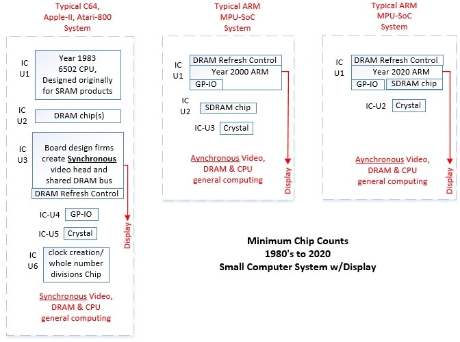
Figure 1, Typical Board Synchronous Designs 1980’s Compared to 2000-2020’s Asynchronous Designs
2.3 Government’s Effects on Products Produced
Automobile designs and electronic chip designs have similar economic and even political forces that act on them. The 1980’s car-maker company AMC created the term “Sport Utility Vehicle” (SUV), for the Jeep-XJ. The acronym SUV is now ubiquitous. And vehicles so listed as SUV’s, are now possibly the most produced model of vehicles today. And SUVs are much to governments’ approval as they find ways to blur the distinction of what is a car or truck, in order to facilitate the acceptance of electric vehicles.
Neither the likes of VW-bug or the Jeep-XJ will come back in new models as they have been fully regulated out of existence by political government agencies. However both vehicle products came into existence from either USA federal law on mileage mandates or German government people’s-car government sponsorship.
In IC-chip worldwide markets, ARM interleave memory Systems-On-a-Chip (SOC), with built in video display, created billions of cell phones. The ubiquitous ARM-CPU cell phone advances the governments’ management of the average person’s texting, twittering and Facebooking, and thus it is here to stay, possibly forever.
On a side note, ARM based cell-phones with “Google Maps” software, and with the phone’s continuous geographic location radio-pings to google headquarters, have created Google Maps products. It is sort of free to the public (in exchange for pinging the user’s geographic location), and acts as the most gasoline (liquid hydrocarbon fuel) saving, and wasted man-hours reducing product in road-driving-traffic history.
Google Maps (typically running on an ARM device) has saved more dollars, reduced more carbon burn, and preserved more productive man hours than the electric vehicles ever have, or possibly ever will. Yet google gets no carbon credits from the government for Google Maps.
2.4 Like DRAM-Interleave, Historical Automobiles Low Cost Leaps Forward
The modern marketplace often forgets the incredible success stories of weight reduced, and cost reduced, vehicles: Two near perfect examples are 1) the Volkswagen people’s car of the 1930’s who’s product line variants ran through the mid-1970’s. The VW-beetle (Bug) even came back in 1998 with a water cooled modern engine, but had lost its low-cost narrative.
And the same story for 2) the AMC-Chrysler Jeep-XJ produced in the USA from 1984 to 2001, and then continued production in China, Egypt, Venezuela, and Argentina for yet more years, with possibly a remarkably large assortment of different engines.
https://en.wikipedia.org/wiki/Volkswagen_Beetle
https://www.motortrend.com/reviews/1998-volkswagen-beetle-2/
https://en.wikipedia.org/wiki/Jeep_Cherokee_(XJ)
Like the Interleave DRAM story in electronics computing design, AMC and VW combined record breaking lightweight unibody design, with simple engines. And they were both product profitability bullseyes.
In desperation to save AMC, minds widened to make new partnerships. The French have a history of introducing nearly forgotten military tank designs for both WW1 and WW2, and new car designs that almost always stressed weight reduction, value, utility and style. France’s Renault Corp engineers in cooperation with AMC designed the lightweight XJ unibody design that ran circles around Ford and GM in the 1980’s. The millions of surviving units of XJ today does not go away as having a lightweight SUV yet rugged design that no other modern SUV manufacturers replicate today.
2.5 History, 6502 RISC CPU Concepts Moved to Romania and UK
In 1984, MOS in the US-State Pennsylvania was probably at 1000 nm. MOS was the inventor, maker, of the 6502, 6510 family. 6510s and 6502s RISC (reduced instruction set) processors of this 1984 era were of the 1000 nm transistor size range.
https://en.wikipedia.org/wiki/65_nm_process
It was the US-state of PA and the EPA who shut down the MOS fab, (pollution is the stated reason). Core knowledge of MOS migrated to the UK, to create the ARM family.
ARM picked up the RISC low cost concept and ran with it. And at first it’s licensing prices were near zero, for IC-houses and fab users. Summarizing this courses.cs.washington_edu link: Acorn Inc ran with the same 6502 design concept, and Acorn became ARM Inc.
https://courses.cs.washington.edu/courses/cse474/17wi/pdfs/lectures/03-arm_overview.pdf
Further discussion here:
And this no-cost RISC processor design concept is still active with new fabless IC firms:
Brief Recap on what “RISC” versus “CISC” instruction sets means, as relating to processor IC’s.
RISC Simple:
- Simple instructions taking one cycle
- Fixed format instruction
CISC Complex:
- instructions taking multiple cycles
- Complex Instructions interpreted by the micro-program
The size of the instruction sets has a large effect on the physical size of the processor chip to be manufactured. As size goes up, it not only uses more wafer, but even more critically, “yield”, that is the number of successful testing chips on the wafer, goes down.
https://www.datasciencecentral.com/profiles/blogs/arm-processor-introduction
China (not covered much in this paper) is making very large and fast investments in chip design and manufacture with the west, who is formally passing regulations to keep fab equipment and technology from China. Russia too is now not just using the Zeleongrad (A Moscow RU suburb city) Fab for its own military chips, but now has commercial world market offerings to include a RISC processor.
Some links for the Russian and China IC Fab race:
https://en.rusnano.com/portfolio/companies/mikron
https://en.wikipedia.org/wiki/Mikron_Group https://www.slideshare.net/TorgpredstvoArg/mikron-leading-semiconductor-idm-company-in-russia
Communist Romania in the late 1980’s copied the 6502 then, and the PC’s that came out of it were the most popular for many years all over the Soviet allied states. Thus there is a large base of experienced 6502 assembly programmers in Eastern Europe and Russia. They can find new interest in new variants of 6502 running at 100MHz speeds (rather than at the old 1.8 MHz of Atari 1984 period) and variants raised up to 16 and 32 bit designs. This effectively creates RISC (reduced instruction set) processor variants, that will compute MIPS at 50 to 500 times the speeds of the old USA production.
It would be illogical for Russia and China to not also make new variants of the 6502. Now, open-source teams in the USA and Europe have successfully reverse engineered the 6502; after all, the Russian’s are at transistor size 65 nm in 2021.
Of these three competing political-economic semiconductor manufacturing zones, China is half capitalist, half command (central government planned/dictated) economy driven. The USA, UK, Continental Europe, being the polar opposite, are probably about 1/4th capitalist, 1/4 socialist/communist, and ½ banker/wall-street-stock-price driven. Japan, S-Korea, Malaysia, Singapore are somewhere in the middle, but like China have a strong bent toward economic nationalism. IC-Fab-companies, geographic and trading-zone group-types, want to avoid a hot war. But the semiconductor war is heating up very fast. Who will win is most likely those that dominate multiple factors of investment, electronics-end-products manufacturing, and a meritocracy of home grown talented engineers.
China, above all other countries in terms of number of engineers and determination, is on a mission from its government to go forth and make chips.
The Russian nation is ramping up IC design and production as best it can at its Zeleograd Fab. China has better than ½ the transistor size of Russia, and TSMC in Taiwan has better than 8 times smaller than Russia and China. TSMC is building plants in the USA. It is yet to be seen if Intel can ever be the company it was in Semiconductor Fab factory operation again. Is this rate of USA Fab factory build fast enough? Mathematically, it appears to not be, and the national determination much less so. At one time, in the mid 1980’s, Washington State was making bi-polar chips in the American Indian named city of Puyallup. It closed, then next it became a Microchip Technology MOS FET fab, then next a Panasonic Fab. Today, the old Puyallup-WA Fairchild Fab (that cost some $400M 1983 dollars to build, funded by Schlumberger of France) is now rented out as dental offices and places to park cable-TV-trucks.
2.6 Semiconductors/Open-Source Competition (Asia-Pacific, CN, RU, EU, USA)
As 2021 wanes toward the 4th quarter and beyond, the international western countries are fiercely feeling the pain of the semiconductor shortage. The effects of the shortage are having domino effects into almost all other industries. The semiconductor “wars”, for lack of a better term, will draw-in the open source chip designs and bring them to new products in a big way.
The 6502 and its companion chips of the Atari and Commodore era are coming back. All those 1970-80’s patents have long-ago run out. It’s very doubtful that copyright infringement of actual chip mask images will have even a tiny effect. There is no business-model to make these tried-&-tested 1980’s netlist designs in 1000 nm, like the year 1985. It’s way easier now to use the 6502 netlists to make these classic 8-bit designs, and/or upgrade them to 16 bit (which has already been done), in 4 nm as at TSMC, or in 65 nm in Russia or 30nm in China. (These nm sizes are noted in September, year-2021).
As a sidebar note, the bigger the transistor size, the more rugged against electromagnetic pulse (EMP) the IC chip is. Larger transistors consume more power, consume more wafer area and are slower. 1000 nm Chip Fabs in the 1980’s that struggled with chip yields from the wafers of a 6502 will hardly do so today in RU and CN at sizes of 30 and 65 nm. It is noticeable that, although RU has historically shared almost all of its technologies with China since WW2, currently CN is not sharing back with RU the smaller transistor size.
The resurgence of the open-source 6502 is likely going to lead a new class of low-cost System-On-a-Chip IC products. It is possible that open RISC-V or 6502 like variants with bus synch-ed video, may end up in FPGA’s as pre-made opensource-IP subsections for ASIC’s.
It is probable that China and Russia subsidize their current chip Fabs. In many ways so do all the other counties. Look for bigger tax breaks to come for the USA and European Chip Fab corporations. It could well be that TSMC leads the way in the USA in coming years, as they have a solid record of fab operations with progressively leading the transistor size shrink-down. TSMC seems to put the value on being a meritocracy, and that may be the key.
3. ARM Systems-On-a-Chip (SOC) Can Improve on Atari/C64 Synchronous Design
There is no contest that ARM bus speeds today dramatically exceed 1980’s 65XX’s based PC products. “Improve” in this context means to obtain better overall product performance for any given SOC chip’s gates and flops that comprise it, and its clock speed capabilities.
Out of box, canned designs from the ARM SOC chip suppliers barely vary from one company silicon supplier to the next, making these chips nearly commodity products. Some have more or less on-board memory, clock speed variations, I/O pin counts, differing numbers of LVDS and HDMI video raster output heads, and camera MIPI-bus input raster heads.
Some of these ARM-SOC’s also include acceleration hardware for video compression, as to be suitable for cameras to store or transmit real-time video streams.
A still open area of the ARM-SOC, PIC-SOC markets is improving synchronization of the video heads and the general computing, audio output, and DRAM refresh. As an example, audio wav-files can be re-sampled to match the horizontal line frequency, and then output the samples, at the same rate of 10-20kHz that well suit audio sample rates.
3.1 Synchronize Simple Sample Audio to Other Bus Processes
Uncompressed audio D/A on the audio output port is somewhat old fashioned, but it saves a lot of audio de-compression MIP’s. This may not suit playing back a 3 minute audio file, but it well suits audio clicks, pings, beeps and whistles needed for products such as cars or cell phones. Small word groups can be used this way such as “door open”, “low battery”, “stop ahead”, “too close”, and with lower latency than that of audio decompression. Horizontal line synchronized audio play-back entirely removes the computing and digital electronics gates/flops acceleration needed to decompress MP3 files.
What is needed for ARMs, PIC’s and 65XX’s in audio playback for blocks of audio sample data is a small address counter, triggered at an audio rate, possibly horizontal scan video-raster rate, that pumps the audio data samples to the audio D/A converter.
3.2 Fully Synchronize the ARM-SOC, RISC-V and PIC-SOC Design Methods
The same applies for ARM and PIC. Here we discuss only ARM to save text. Both ARM and PIC today are typically sold as Systems-On-a-Chip (SOC), yet largely ignore synchronizing the video raster process, camera raster process, audio-data-stream-process and DRAM refresh functions.
By processes-and-functions synchronizing, it can be possible to drop the overall clock rates, or data bus width, possibly by half. The reduced ARM processor and DRAM member potency is possible in that the software programmer, whose task it is to make that hardware board in an end-product behave from a DVD player to a Climate-Map system in a automobile, won’t have to deal with the unpredictable loss of memory and processing cycles at unknown times.
Saving bus Flip-Flop/gates transistors and their state-transitions further saves electrical power, and further saves cost. Expect further savings in validation test periods due to the deterministic timed behavior of the product’s main duties of:
User software applications compete for processor and memory cycles against:
* video display raster process, * camera input-raster process,
* audio-data-stream-process and * DRAM refresh functions.
The overall product performance worsens in general if the processors are asynchronous. The simplest way to make an ARM SOC fully synchronous may not be to reinvent the wheel. Rather, copy these early late 1970’s and 1980’s synchronous methods of those older systems, like older 8-bit PC or video game machines, whose primary bus-data-reads duty was to feed the video CRT display a perfect repeat video data stream.
Very fortunately for the modern electronics designer, are two improved main factors of:
* 1) LCD and OLED displays being much more forgiving for video timing requirements than CRT’s, and
* 2) DRAM refresh is already built into the ARM; it just needs some modest improvement.
That makes the ARM-SOC full product synchronizing process achievable.
Both of the two factors above can be addressed in either the SOC chip at the chip design firm, or by the board designer, working in concert with the software/firmware engineer.
3.3 Two 1980s Video Raster Engines, Applied to ARM SOC Synchronous Design
Atari’s 400/800/1200 6502 and Commodore C64 family products were fully synchronous designs based on RS-170 video timing. Thus NTSC and PAL Atari’s & C64’s had slightly different clocks, and needed small changes in firmware, across multiple world regional TV-display markets of NTSC and PAL.
The C64 was a fully synchronous design, based on RS-170 (NTSC base-band) video timing. The C64 ICs however, as they compete for memory cycles, crossed a DRAM refresh timing boundary that from time to time, resulted in memory corruption due to a meta-stable like, data bus events.
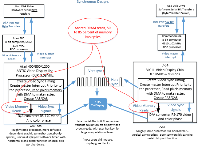
Figure 2, Atari and C64 Used Custom IC’s for Video and DRAM Refresh
The 1980’s designed sections for custom video, custom sound, custom peripheral IC’s were connected to Commercial Off The Shelf (COTS) CPUs (originally only able to work with SRAM). This group, of custom and COTS make up the 1980’s system design were divided up into subsections. The subsections then were interconnected with glue logic, built into the custom chips, wherever IC size would allow.
At the end of the chip design process, various leftover parts, not in chips, are put in those chips that still have spare pins and spare silicon area budget for a little bit of growth. The majority of the fanciful functions in the chips, are then turned into acronyms for Custom IC marketing names.
3.4 Which Process Gets Memory Cycles when DRAM-Refresh, CPU and Video Compete?
When Atari-800’s are in high-res video mode (4 colors, 320×200) video consumes most of the memory bus bandwidth.
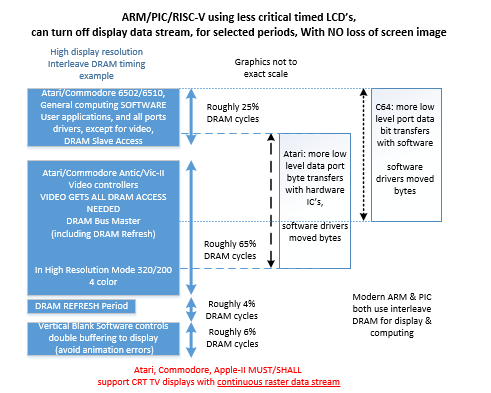
Figure 3, CRT-TV-sets of 1980’s Required Critical Timing in Almost All Cases
Likewise the same was for the C64, high-res means that video consumed most of the memory cycles. In low-res modes, the software user applications process could have 80% or so of the memory cycles.
Late models of both the Atari and Commodore PC’s had the ability, for the user, to turn off the CRT display raster pixel data stream, by only providing RS-170 video sync signals with a flat background color, while large computing tasks occurred. This would have some equivelencey to the ARM use of Gated-Clock-OFF to the video-raster-output section, except that there is no default circuity to make keep-alive sync’s to be sent to the display.
3.5 DRAM Priority Switches 1000s Per-Second in Classic Random Hardware Control
Still, in both Atari-800s and C64s however, the swapping from video memory reads, to processor general computing R/W access of memory, typically flipped back and forth thousands of times on each full screen raster. And this is what ARMs and PICs also do in modern times. The swapping is mostly an indeterminant (semi random) process that is kept inside some timing boundary limits. DRAM (Dynamic Random Access Memory) in general needs to have memory access for DRAM-Refresh function about every 15 usec.
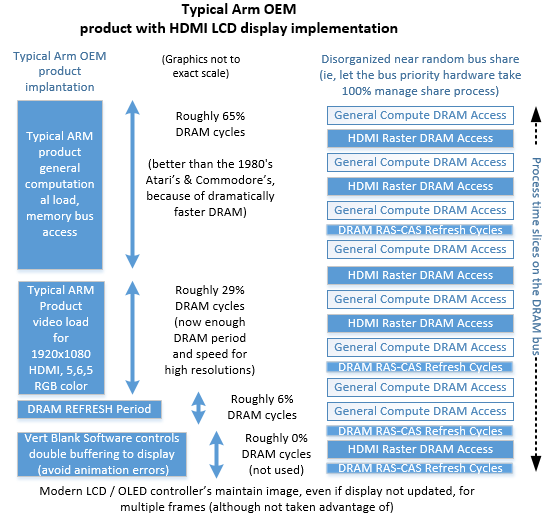
Figure 4, Typical Semi-Random DRAM Refresh, to Software Application Timings
Due to this bus priority switching, the programmers of the 1980’s needed to carefully plan their assembly code for a video game. But at the same token the programmer was given all new functions like Display List Program (DLP) that was code they could tinker with that changed the setup of the video controller on every horizontal line if desired. DLP method was used very often in award winning games.
But the thousands of times per sec of DRAM control being taken by video-process hardware “stealing” from the C64-6510 or Atari-6502 processor, meant that at when in high resolution video, the programmer could not plan as well as desired, the absolute execution period, of code such as 10 lines of assembly.
Disk or Cassette I/O would suffer some slowdown with high-re video. Time delays on the 65xx PC’s firmware, especially as DRAM access interacted with the delays in the peripherals, could behave as almost random.
3.6 DRAM (1980s), SDRAM (1990s) and RAMBUS (2000s) Years Variations
The 65xx microprocessor was conceived with regular Static-RAM (SRAM) in mind, as no companion chips for DRAM management came from MOS-Inc when the first 6502 was released.
This section acts as reference to DRAM types of the 1980’s to present, as to compare refresh methods.
Classic DRAM of the 1980’s where for a single strobe of RAS (row) , could be followed by multiple strobes on CAS (column) addresses as the fastest change to the next 6-bit column address in memory. It was that 1980’s Refresh Procedure that the end-product company had to make for itself, with either COTS logic chips and Programmable Logic Array (PAL) or a custom chip. SDRAM does much of that for the processor designer today.
https://www.acornatom.nl/sites/fpga/www.howell1964.freeserve.co.uk/projects/dram_6502.htm
[Hardware / Software K. Howell 6502, two 64Kx4 DRAM chips, TTL logic.
Published Electronics Today International, 1985, At the time of this project (1984), memory was expensive. The home computer boom (pre IBM PC) saw a proliferation of many different computers. …The 6502 (in this Atari example) does have one significant advantage: the memory access cycles are very regular. The 6502 has a single clock output with a 50% duty cycle.]
(Timing graphics of 6502 PH2, PY2′ RAS, MUX, CAS in this published write up by K. Howell is an excellent example of 1980’s DRAM timing, in a real world implementation.)
https://www.tomshardware.com/reviews/ram-guide,89-5.html
[accomplished by activating the column address buffers on the falling edge of RAS\ (rather than CAS\). Since RAS\ remains low for the entire page cycle, this acts as a transparent latch when CAS\ is high, and allows address setup to occur as soon as the column address is valid, rather than waiting for CAS\ to fall.]
https://en.wikipedia.org/wiki/Dynamic_random-access_memory#Page_mode_DRAM
[Page mode DRAM is a minor modification to the first-generation DRAM IC interface which improved the performance of reads and writes .]
Circa 1986: [ Tex-Instrument Data sheet TMS4500A Dynamic RAM (DRAM) Controller User’s Manual]
https://www.datasheets360.com/pdf/-1862440600650638492
Circa 1986: [Micron data sheet MT4264 64K x 1 DRAM with page mode]
https://whatis.techtarget.com/reference/Fast-Guide-to-RAM
quick list of all RAM memory types, 1980’s-2020’s: Static-RAM, DRAM, FPM-RAM, Enhanced DRAM, PC66-SDRAM, PC-100-SDRAM, JTAG-DRAM, DDR-SDRAM, Direct-Rambus, GDDR…
https://www.exxoshost.co.uk/atari/mirror/myatari/issues/may2002/dram.htm
These SDRAMs (Synchronous DRAM) dominate today’s memory market. In basic principle this memory species works exactly like the memory types described above. Nevertheless SDRAM is appreciably more flexible and intelligent than its predecessors. All control signals depend on one clock, which – according to the age of the SDRAMs – may be 66, 100, 133 or at present 166 MHz. The control signals themselves (/CS, /RAS, /CAS, /WE) should be understood as a kind of command issuers which tell the memory exactly what it has to do with various bit-patterns. The SDRAM stores the present command during a rising clock edge. It is so advanced in its construction that after receiving a command it can perform the task assigned to it by itself, without requiring further external control signal.]
https://www.realworldtech.com/rambus-basics/2/
[In contrast (to DRAM and SDRAM, the Direct Rambus memory system is arranged logically as a single long strip of DRDRAMs consisting of up to 3 RIMMs and 32 devices per channel. A common 16-bit wide datapath serpentines around the motherboard, entering and exiting each RIMM in the system until finally being terminated. ]
Today ARM Cortex-M3 uses the SDRAM memory interface.
https://class.ece.uw.edu/474/peckol/doc/StellarisDocumentation/IntroToCortex-M3.pdf
https://arcb.csc.ncsu.edu/~mueller/ftp/pub/mueller/papers/ecrts10.pdf
[Making DRAM Refresh Predictable, Balasubramanya Bhat, Frank Mueller, NC State University, Raleigh, NC. …..
The basic idea behind both approaches is to remove the asynchronous nature of hardware DRAM refreshes.]
See this csc.ncsu.edu white paper detailed in “ARM-SOC Synch DRAM Refresh Method” section.
3.7 ARM Gated-Clock Power Savings Method and FlexBus (NXP)
Some ARM-MPU-SoC variants at present use a form of “Flexbus” (marking term from NXP) that is a type of synchronous main-bus of the ARM whereas the CPU/MPU-SoC (system on a chip) and the Raster Engine run at whole number divisions, of clock speeds. The Flexbus clock speeds are selectable, in whole division numbers, for those busiest hardware processes that access the main memory bus that also cross clock speed boundaries
Many of these same ARM variants have a timer controlled approach to shutting down selected clocks, such as the video raster (aka LCD video engine), that can completely turn off , by shutting off its clocks. SDRAM will continue to be refreshed, but the main display, and its needs for pixel-data-memory reads, can turn off.
The software commands to Gate-Off the pixel clock to the raster engine, is a video shutdown method, albeit not very exact in timing control, to accomplish phase-locking an ARM video product to an external video vertical sync signal. The Gating-On command can be triggered by an input pin, or internal timer of the ARM CPU, via an IRQ or polling process, thus video output is returned to ON-running mode.
Some schools of VHDL and Verilog discouraged designs with gated-clocks, as sort of deleterious to classic programming language style. However if used in limited locations, it is a powerful component in a design. However this view is changing, and is in mass production IC’s, example links/excerpts below.
[using the MUX enable to gate the clock signal of the flip-flop via an inserted clock-gating element]
https://pdfs.semanticscholar.org/b3f7/0546533fc3d548f5b422abb693244573adc6.pdf
[A New Clock Gated Flip Flop for Pipelining Architecture, K. Raja, S. Saravanan, Shmuel Wimer
proposed on VLSI chips have Gclock (gated clock) signal in these days a mainstream design methodology for less switching power consumption]
https://www.nxp.com/docs/en/data-sheet/IMX6SDLIEC.pdf
[i.MX 6Solo/6DualLite Applications Processors for Industrial Products (with 1080p video out)
Flexible clock gating control scheme…….. 4.11.10.5.1 Synchronous Controls
The synchronous control changes its value as a function of a system or of an external clock.
This control has a permanent period and a permanent wave form]
4. Atari Example, Display Raster Reads, Optional Turn-Off Video, applied to ARM
In synchronized systems with video-out, the basic design tenant is that the video pixel clock will be the most important clock speed of the system, and that the main CPU clock, will be adjusted, typically in the range of 10%, up or down, to be whole number (such as 2X, 4X) multiple or division 1/2, 1/4, (some video pixel FIFO’s may still be used in such a system to aid in the final video buffer, pixel-data-stream-speed rate, before display, possibly as long as a horizontal display line).
These adjusted clock speeds for the benefit of the video raster display engine, would require home computers of the 1980’s to have slightly different CPU clocks for the North American NTSC CRT-display market and the European PAL CRT display markets.
This link describes the Atari video controller, in how it would halt the processor to take control of the shared synchronized memory bus.
https://playermissile.com/dli_tutorial/ (text copy from Atari WhitePaper] )
[“ANTIC is the special coprocessor that handles screen drawing for the Atari computers. It is tightly coupled with the 6502 processor, and in fact can be thought of as being the driver of the 6502 because the ANTIC can halt the 6502 when needed.
Since only one chip can read memory at any time, ANTIC needs to halt the 6502 when it needs access to memory, so this Direct Memory Access (DMA) can cause 6502 instructions to appear to take more cycles than documented in a 6502 reference.
In fact, the amount of time ANTIC “steals” will depend on many factors: the graphics mode, player/missiles being used, playfield size, and more.”]
Above note the (Atari) “ANTIC (the display raster chip) needs to halt the 6502” this is because CRT RS-170 display sync, and analog brightness/color signal timing must always be perfectly periodic or the old fashion CRT display systems would otherwise fail to display the video stream data.
Thus “can cause 6502 instructions to appear to take more cycles than documented in a 6502 reference”.
This was also commonly called (memory or bus) “cycle stealing” when the video processor had priority over general purpose computing. Same is the case for all 65XX variants.
The deleterious effects of this can be experienced in semi-random slowing of the software apps. Video display stolen bytes cycles, if they happen at the same time as other critical general purpose computations, especially for servicing other hardware ports, could cause a timing hiccup on a hardware port, long enough to cause a data error, on a disk-drive port, printer port, joystick port, or RS232 port.
A common solution in the 1980’s was to slow down the hardware port communication speeds, until the data errors stopped. Some models of the C64 lived with DRAM R/W refresh errors, and slowing down the CPU helped. For both C64 and Atari, they had some issues of unpredictable cycle counts in some gaming software’s due to the video bus cycle stealing.
4.1 Atari/C64 Versions Hot-Key Turn-Off Video Raster Memory Reads
Late model Atari’s and Commodores could Turn-Off video, and just “blue screen” while a large program ran, such as searching a database.
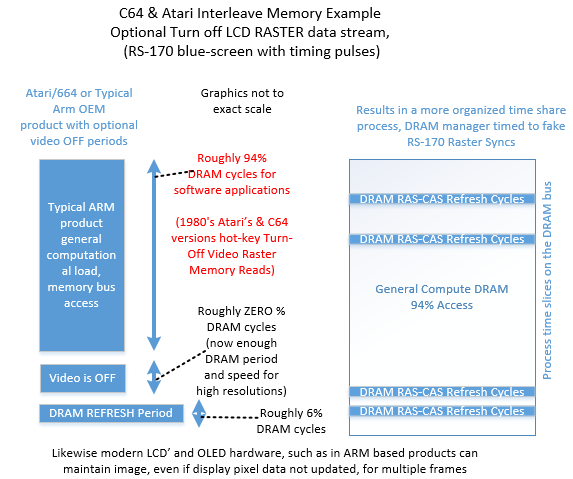
Figure 5, Atari & C64 Late Models Optional Video Raster OFF
ARM-SOC’s can also Turn-OFF video (like Atari did to give all memory cycles to the processor) , and as such create the cycle sharing map as the one below, where only DRAM refresh is stealing memory cycles. This is where the timing-generous and easy to use modern LCD and OLED displays are desirable. These displays can keep an image on the screen when the raster stream is turned off.
Some LCD displays going back to the early 2000’s decade that did not have a memory chip, could also have video data stream Turn-OFF for a frame. The capacitance thin-film LCD transitions per color dot, held their value long enough that it was not noticed by the viewer, as there was no visual change.
Most modern LCD’s exhibit the sample-hold effect. This can vary, more expensive the LCD’s, are more likely to fight the designer to use novel timing, to skip frames of refresh. Avoiding a vertical next sync may allow some LCD’s to retain the present image for a long time, such as server frame times.
“testufo” web site shows the animation rates of 15 FPS, 30 FPS and 60 FPS. The designer should not be planning for an animation faster than they are updating the LCD or OLED.
“Sampling method, Impulse vs sample and hold, Any long-term CRT users, particularly gamers, will recall that there was a distinctly different feel to gaming on a CRT. Modern LCDs have generally rapid response times and high refresh rates which certainly help reduce trailing and perceived blur. But still there is something missing.
Objects that remained sharp during brisk movements on the CRTs may seem relatively blurry on even the fastest LCDs. ……… There is a distinct difference between how CRTs and most LCDs sample images. It is this that is the missing piece of the jigsaw and the major factor in perceived motion blur.
LCDs and OLEDs typically adopt a ‘sample and hold’ (or ‘follow and hold’) approach to displaying an image whereby a frame (sample) is displayed to the user until the next frame needs to be drawn (hold). “
https://www.nelson-miller.com/what-is-image-persistence-in-lcds/
“Image Persistence: the Basics
AKA known as “image retention”, and “image persistence” is a phenomenon in which the image of an LCD remains visible after the device has been turned off. The good news is that image retention is temporary and usually reverts back to its original, default state. This is in stark contrast to the “screen burn” of plasma displays, which are typically permanent. Nonetheless, most users prefer to avoid the visual imperfections of image persistence”
From T.I. (LCD persistence can be so long, it can be quite problematic to small desired image changes.)
https://www.ti.com/lit/an/snla185/snla185.pdf
“This is due to several factors including that computer applications typically have very low video content and what little video content there is tends to be poor quality (e.g. internet video streams, file based video clips and game graphics).
Furthermore, the LCD industry specifications report only the off-to-on response times of the panel. This is the fastest response mode of the liquid crystal. Response times of 15 to 25 milliseconds is representative and would be adequate if all gray-to-gray transitions were at this rate. However, the gray-to-gray response times can be many times longer, i.e. hundreds of milliseconds. These gray-to-gray transitions account for the poor quality of motion video when it is due the LCD response time.”
The LCD’s ability to Turn-OFF updating a raster frame or frames to the display, is usually not documented in the LCD technical specification sheet. Even the technical representative is unlikely to know this information. Often it requires lab experimentation to check this on a raw LCD.
4.2 ARM-SOC Sync Hardware-Software Processes Better than Atari/C64 (M-1)
This method 1 takes over making its own video turning syncs and banks, and both turns HDMI video raster off (command register in the ARM) Gated-Clock-Command (GCC), and additionally turns the HDMI video raster back on.
All the while, consistent periodic timing is kept by the ARM’s timers or an external timer, to match what would be a standard 60Hz LCD refresh. Tristate buffers manage the external syncs and the ARM supplied HDMI raster syncs. Note the designer needs to determine if their particular LCD needs the syncs to stay running, or it is better to turn off. And save more circuits.
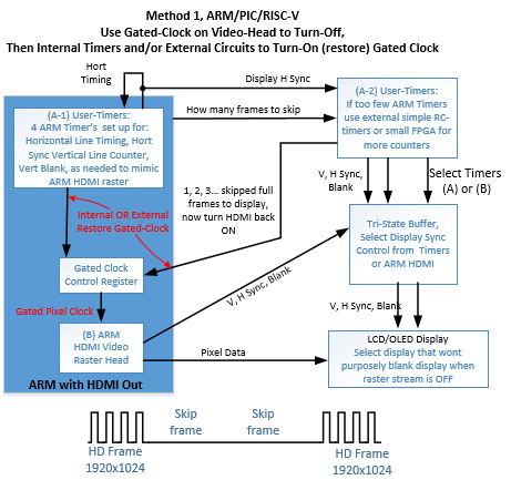
Figure 6, Gated Clock used to Extend Vert-Blank from VESA Standard Timing
The designer needs to be aware if the raster memory map in the ARM-SOC was updated, and does that update need to be presented to the viewing user? Depending on the product application, this method can also be used rather than double buffering of video, to create smoother animations.
This M-1 method can be applied to multiple System-on-a-chips, no matter if, ARM based, If 6502 based, it would be done with a new IC that mimics the old Atari ANTIC or the Commodore VIC-II, upgraded for a larger memory map. Or it can be done with external FPGA circuits that can “phase lock” (both to be both synch-ed and in-phase) to multiple video raster engines, input or outputs. Further see this whitepaper section “pixel clock subtraction phase lock process”.
4.3 ARM-SOC Sync Hardware-Software Processes Better than Atari/C64 (M-2)
In method 2, no external timing was needed for the LCD or turning the ARM’s HDMI raster back-On.
This would be the cleanest lowest cost method for build and power savings. However it is non-standard to the published VESA timing. Depending on your LCD display part selection, the designer may or may not be able to do this.
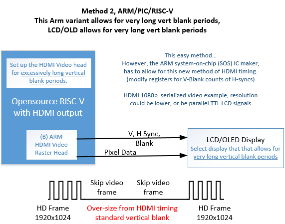
Figure 7, Long Vert-Blank Via V-Blank Register Changes (variation from VESA Standard)
4.4 ARM-SOC Sync DRAM Refresh Method
In this method, after video, and optionally sound, using simple sample file methods, has been fully synced, DRAM refresh is also turned OFF (an ARM register), then turned back on by timers. Thus DRAM refresh is kept in a vertical blank period, and as a planned process, the software programmer designs for.
An in depth DRAM refresh white paper has addressed these DRAM refresh asynchronous timing concepts
https://arcb.csc.ncsu.edu/~mueller/ftp/pub/mueller/papers/ecrts10.pdf
Reference White Paper Title: “Making DRAM Refresh Predictable”
[ A typical DRAM requires one (portion of the) refresh cycle every 15.6 µs…..
……….. entire DRAM is refreshed once every 64 ms ]
( 15.6 us is a typical horizontal line video display sync period)
(16 ms equals a typical 60Hz vertical video display refresh rate)
[ In general-purpose computer systems, the delay due to DRAM refresh has no impact on program correctness and little impact on performance. Embedded control systems deployed in safety-critical environments or process plants, on the other hand, generally impose more stringent timing predictability requirements that are prone to be violated due to DRAM refresh delays .
From avionics over industrial (chemical or power) plants to automotive subsystems such as ABS.
Determining the execution budget by bounding the worst case execution time (WCET) of a task’s code is key to assuring correctness under schedulability analysis, and only static timing analysis methods can provide safe bounds on the WCET (in the sense that no execution may exceed the WCET bound) [23].
….. However, none of these techniques consider the effect of DRAM refreshes on WCET bounds. Hence, a statically derived WCET bound is only safe if augmented pessimistically with the cost of refresh delays, which is inherently difficult to calculate or even to tightly bound due to the asynchronous nature of refreshes combined with task preemption……
……. The basic problem with the hardware-controlled DRAM refresh is that the periodic refresh events generated by the DRAM controller and the memory access events generated by the processor are not synchronized with each other.
Whichever event comes later will have to wait for the former to complete. .. interleaving refresh operation delays the next memory access. The central idea …. is to remove the asynchronous nature of the two events and schedule the two events at predetermined time intervals so that they do not interfere with each other.
…..we describe two methods to perform DRAM refresh using this approach. ]
The hardware designer needs to check closely their specific DRAM IC Refresh time limits timing specifications. Also the designer can operate DRAM refresh timing faster than the DRAM maximum no-refresh time-limit specification, to make up for the 1/60 th of a second DRAM refresh was not on. Fast-as-possible DRAM refresh full-cycle can be completed in the range of 1/1000 th of a second, continuous, at the bottom of a video frame.
In a relatively slower clocked ARM-SOC, this design can also include control of DRAM refresh, whereas the display could go into a high display resolution or the processor performs some critical computation with no unexpected DRAM refresh occurring, at a critical memory bus share high-load event.
More quotes’ from this excellent white paper, csc.ncsu.edu (authors email bbhat@ and mueller@) where the writers also contributed considerable lab test man-hours. [ A Distributed Refresh in Hardware, In this method of refreshing DRAMs, a single refresh operation is performed periodically, as illustrated in Figure…. ]
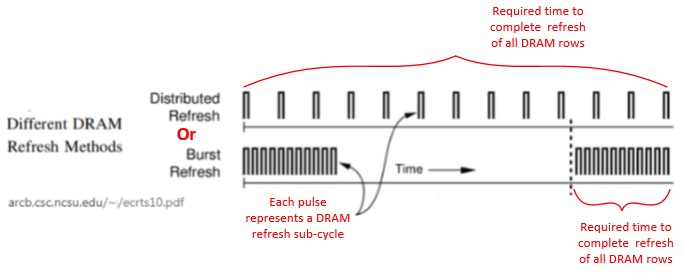
Figure 8, Burst DRAM Refresh Under Board Designer’s Control
For additional clarity, red lines and text added to the ncsu.edu white paper drawing above. Once a full cycle of refresh is complete, it is repeated again starting from the first row. This is currently the most common method for refreshing DRAMs. This can draw a higher instantaneous power-current burst, on the DRAM VCC, but should not change the overall amount of wattage to complete a full refresh cycle. NCSU white paper quotes continue below.
[…we describe two methods to perform DRAM refresh using this approach….
A. Software-Assisted Predictable Refresh
B. Hybrid Software-Initiated Hardware Refresh…
…….We implemented our methods on three different embedded hardware platforms
…….The third (test) platform is a IBM PowerPC 405LP evaluation board which is used exclusively for the SDRAM energy measurement experiments.
…….We observed that the workload takes exactly the same amount of time in every iteration. This is because the on-chip SRAM does not need periodic refreshing and exhibits uniform latency every time it is accessed.
…….At every invocation, this task refreshes a subset of rows using our hybrid refresh method. Figure 6 (of ncsu white paper) compares the energy consumption of the SDRAM at different load points (from 10% to 90%) between our approach and (standard built into popular ARM chips) hardware more automated refresh. As can be seen from the graph, our approach always consumes less energy than the hardware auto-refresh method. We obtained about 5% energy savings on the average
…….Experimental results
confirmed that both methods result in predictable DRAM accesses without additional refresh delays. ….. Overall, our new methods alleviate the unpredictability of DRAMs due to refreshes, which facilitates design of hard real-time systems with DRAMs in an unprecedented manner.]
The Reference White Paper Title: Making DRAM Refresh Predictable” with web-link , https://arcb.csc.ncsu.edu/~mueller/ftp/pub/mueller/papers/ecrts10.pdf
agrees with the recommendations here for both the ARM’s and PIC’s that have hardware DRAM management built-in, but can benefit from user implemented board and software designs that add more synchronicity to the ARM DRAM refresh and video head memory-read operations.
And is also the case for the old 65XX family processors, which are now having a new resurgence due to open-source reverse engineering of netlists. The 65XX family did not have any DRAM management build-in, nor built-in video controller heads.
This rare 65XX open-design in these modern years, of combining FPGA’s, and ASIC’s with CPU chips, makes the 65XX even stronger candidates (than ARM and PIC) for video heads to be added, that manage DRAM in an extremely synchronized manner.
The proposed extremely synchronized CPU and Video functions of R/W in DRAM attached to the 65XX processors, can produce lower cost, lower clock rate, and very capable products, and even those products with critical I/O timing.

Figure 9, Synchronize Audio Samples on H-sync, and Burst DRAM Refresh
4.5 ARM-SOC Memory Interleave Combined with Synch Methods Summation
Multiple techniques can synchronize almost any process/machines. ARM-SOC are well positioned to take on this game-machine like behavior for improved performance with use of slow clocked ARMs.
Interleave memory ability that is designed into most ARM at the chip level make them good candidates for game machine design, even if not at all used as a gaming device. Wherever computers have displays, the users need to see screen updating in a natural smooth manner frame to frame. Either ARM family chip designers, or board designers can use synchronized raster methods. The reverse engineer open-source groups are publishing the 6502, Atari and C64 chips sets netlists on the world.
5. Pixel Clock Subtract Phase Lock, Video Feedback Loop, Multimedia ARM
Another method to synchronize, or more accurately stated as phase lock, is to control not only the repeating rate speed, but also the repetitions phase, of process-A to process-B, exactly aligning temporally (synchronizing).
The clock subtraction method (free, US-patent 6,262,695 has expired) is easily added as a few gates, making the use of multiple, slower clocked SOC’s able to become larger, more potent, multi-display chip products. See the Mimax.com website for more white pacers to install (instantiate) the gates/signals of clock subtraction to phase-lock many repetitive digital processes. Video sync (a.k.a. Vertical Phase-Lock, or V-Lock) via this 6,262,695 method is like ARM’s gated clock method, but functions on a repetitive, periodic automatic mode, versus software commanded Gated Clock.
In the timing diagram for clock-subtraction on two video heads, can also be allied of any number of video and camera heads. Cameras and video display can be purposely phase shifted to opposite phases of a repeating period, and thus also accomplish no display image tearing of the camera images, and yet no double buffering is necessary, further reducing bus loading.
Pixel clock subtraction for a multimedia processors on an ARM SoC, RISC-V SoC, 65XX system, PIC-SoC or any multi-head graphics card, to work with a mere two gates, one XOR and one NAND, the two sync signals need to be of the same number of clocks in width.
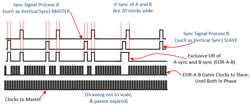
Figure 10, Pixel Clock Subtraction to Gently Phase Lock, Avoiding DRAM Refresh Loss
In multi-raster display head systems, such as higher end cost ARM, or a dual-head video-graphics card in an X86 PC, are typically, not-in phase lock, (MiMax inc video on youtube has O-scope signals clock subtraction) out-of-phase condition of two-display-heads. Even when both heads are at the same display settings, vert-rate, and pixel-hort-count, and vert-line-count, resolution, and with same pixel clock, from the same clock crystal & PLL, the two heads are persistently out of phase, and at random phase positions each time the system is booted up.
Typical dual head video cards, the video driver software sets up the registers in each display head, first one display head, then the next display head. The video card software driver can be interpreted by many operating system processes and other hardware driver software, randomly during boot-up. Thus the random, head-to-head phase condition when operating.. Some video card OEM’s have made dual head GPU’s that can send a sync-re-start signal to the video heads timing engine and its address synchronous counter, and this will get the heads in sync at boot up time. However that method still lacks a function of detecting a phase lock loss, and for regaining phase lock without a large video artifact hiccup to the display(s). Sync-Phase lock test’s and shipped products have been with multiple-GPU chip’s (single head in each IC) phase locked, and with deal-head-GPU chip, (with both heads, in one GPU) phase locked up to SXGA displays, at 75Hz vertical refresh rate, and over 100MHz pixel clocks.
Clock subtraction, as noted, can be applied to many periodic processes, here we call it Pixel Clock Subtraction (PCS) (for video uses the marketing name V-Lock, aka Vertical Lock) when applied to two video heads of the same resolution, and same scan timing, and same source clock, except where the slave video head clock is gated, via an EX-OR of the V-sync signals.
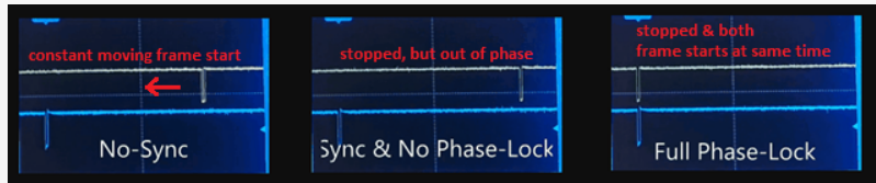
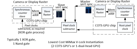
Figure 11, Pixel Clock Subtraction O-Scope Images and Dual Display Example
Below is a link to a Mimax white paper showing a dual head video graphics card, that has the PCS turning Off and On, for demonstration. The “auto-industry” whitte paper has a Motion-GIF of PCS (V-Lock)
https://mimax.com/tag/auto-industry-white-paper-phase-locking-of-mems-hud-system-video/
Or can be seen in the youtube video
Phase Locking Value (PLV)
https://journals.plos.org/plosone/article?id=10.1371/journal.pone.0146443
[more accurate estimations of oscillatory synchronization across a wide range of different synchronization regimes]
Pixel Clock Subtraction, (PCS/V-Lock) will auto-detect and regain phase lock, and with no visual glitch or hiccup to DRAM refresh (if DRAM memory refresh, or video GPU DRAM registers, are synch-ed with horizontal blank)
MiMax.com website has more white papers to assist with designs that can benefit from periods of video display-off, the Mimax patents of video-raster memory-change hardware-detection does that task, with low cost synchronized raster feedback loops in SOC’s equipped with dual video head, and camera input port .
- US Pat No. 8,139,072 Network hardware graphics adapter compression (video feedback loop)
- US Pat No. 8,441,493 Network hardware graphics adapter compression (multiple video feedback loops)
- US Pat No. 10,499,072 Macrocell Display Compression Multi-Head-Raster-GPU
- Free (expired), US-patent 6,262,695 V-Lock (pixel clock subtraction).
The Mimax Network hardware graphics adapter compression (note above), has some similarity of the ARM Frame-Buffer-Compression patent (aka AFBC, from Arm inc. Rather than from the SOC chip to the display inches distance, it can prevent re-transmission of display data on both a pixel or maco-block level, locally (inches) to world wide geographic distances. Hardware feedback video loops are detailed in separate Mimax white paper.
5.1 Sync and Phase Lock Display-Raster-Out and MIPI-Camera-Input of ARM SoC
Pixel Clock Subtraction (PCS), is a method that gently brings multiple digital periodic processes into phase lock of a master, by gating only a few clocks off at a time; this is a more gentle process as not to interfere with DRAM refresh, than the ARM Gate-Clock Command (GCC) method.
In some cases DRAM refresh that is sometimes not well described in data sheets of ARM and PIC processors, can have its clock dependent on other processes. This is also the case with pixel clocks in some GPU chips, whereas non datasheet detailed DRAM refresh can be pixel clock dependent.
PCS automatically recovers phase lock if lock is lost, and a latch can grab the XOR gate condition to monitor if phase lock has been lost. ARM GCC recall requires a software command to initiate it, and another software command to turn the clocks back on. GCC with software involved, only a near phase lock can be established. Thus the number of cycles involved to measure relative phase lock quality can be extensive, and basically is not practiced with the ARM GCC method, except for power savings.
PCS can clock with an accuracy as the width of a single clock pulse, and is typically the better method to further do functions of real-time pixel data boolean logic testing/comparing of multiple video rasters. If two camera heads are frame phase locked (to the accuracy of pixel timing) then some power hungry video FIFO’s can be avoided.
Comparing the two camera heads, any searched-for pixels matches, or pixel differences, as for processes such as stereo (dual-head, dual lens) camera systems, is the 1st MIPS intensive process that is looking for which pixels in the image, represent near (closer) pixel objects, and simultaneously which pixels represent the fastest pixel moving objects. Stereo cameras of this nature can in many cases handle object real-time distance determination as well as more costly LiDAR. PCS can also be used for transparency overlay of multiple rasters, such as lines/text on top of moving camera display.
Below are several timing diagrams of using pixel clock subtraction for ARM-SoC, RISC-V-SOC or any other processor system with multimedia of video out and cameras. First is the example of a system phase locking and blanking video out, and counter-phase clocking in the camera input data.
In the case of a multimedia system, where the designer cannot gain access to the (A) display raster pixel clock, or ARM-Gated-Clock, or the (B) camera MIPI head not having an external raw clock input, or sync input, a phase locked system is still possible. If just either the video-output head can be locked, or the video-input head can be locked, then that one can be the slave timed process.

Figure 12, Phase Locked Long Display V-Blank to Camera Inputs
For a stereo system the MIPI camera system, the two camera heads would need access to a sync input pin, or the pixel clock, as in the timing diagram below. And preferable to also phase lock the video display raster engineer to a counter phase, to obtain inherent display camera image double buffering like effect.
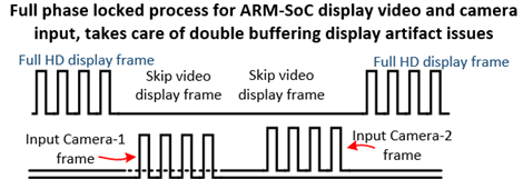
Figure 13, Phase Locked Stereo Input Camera Timing
- Conclusions
Like the 6502 Reverse Engineering (RV) netlist open-source-project, likely to follow are more RV open sourcing of the C64 VIC-II, and the Atari ANTIC video controllers, via the open design organizations of EU and the Americas. Open-sourcing of these old companion synchronous video chips (in progress) makes creating new ARM’s and 6502 variants, as System On a Chip (SOC), a high probability.
https://hackaday.io/project/165624-mocka65xx-universal-650285xx-cpu-replacement
The open-source movement may have unique opportunities soon. One Fab and design center is basing its business model on open-source everything from IC-netlist to production fab-equipment design, is Interuniversity Microelectronics Centre (IMEC), aka “the Switzerland of semiconductors”, located in Belgium.
Internet linked groups are expanding information on 6502 chip history, programming and end-products.
It can be requested of the 6502 8-bit SoC comeback processor designer engineers, to add three items: A) The famous Zero-Page fast memory addressable section of the 65xx memory map of 256 bytes, would be to add 256 bytes of internal cash-SRAM, and to allow the processor to run internally, with that tiny cash SRAM, rather than fully halt all function, while DRAM bus is prioritized off of the CPU. B) Duplicate the 6510’s GP-I/O 6-bit port pins that are on the CPU bus, but would also stay active, while DRAM bus is prioritized off of the CPU. And C) like the last years of the Atari and Commodore 8-bit PC’s, to allow for 16-bit address-bus bank switching, for more 64K-byte memory banks, all in a popular size SDRAM chip. (banked add-on memory was often used as a RAM disk).
The lean-design concept RISC-65xx, including both 8 and 16-bit variants were very widely used, and it is likely to have a strong resurgence due to open source designs and the large base of experienced programmers. With so many teams worldwide now having open-source net-lists, open-source emulators and open-code VHDL variants, the production of these old chips, new design variants, with more registers, wider data buses of 16 and 32 bit, and higher clock rates will follow.
The 65xx re-make as a SoC IC product would need a GPU for video-out, camera-in, audio-out, and DRAM management designed for it. It would be a marketing mistake, to make the video in/out functions asynchronous, as is so many vanilla ARM, PIC, RISC-V variants. Various methods can provide genlocking, or ability to phase-lock to external video, in a new 65xx SoC that would add a unique feature, to pull yet more products to use it, such as multi-display system automobiles.
With yesteryear RS-170 CRT, perfect periodic raster data stream timing was needed. Modern displays of LCD and OLED types open new possibilities to not continuously raster scan. Also to have optionally very fast display updates of whole frames, and very long vertical blank periods.
Optional, and easy to design in, phase locking (both to be both synch-ed and in-phase) multiple SOC’s video raster engines is possible, making the use of multiple, SOC’s able to become larger more potent, cross-commutating, multi-display/camera products. Synchronous IC timing of CPU with display removes the most common Asynchronous bus events in most SoC’s with display. Thus speeding up bus data movements, where meta-stability issues do not then require more series D-flops and faster clocks or more clock phases, as a fix.
Turning off raster scanning temporally in synchronized general-purpose-CPU/video chip (custom or ASIC) or product designs can cost-reduce, and recover significant percentages of CPU and memory bus time, otherwise lost. Synchronous Video display, and camera inputs, will likely become a more common design method with the coming variants of the current ARM family and the resurgent open source, old and new processors.
Synchronizing DRAM refreshes better with video raster timing, can produce 65XX, RISC-V, ARM and PIC Systems-on-a-Chip (SoC) lower cost, more deterministic timing, and allow for larger transistor sizes to be made in Fabs in RU and CN. This paper reviewed multiple methods of Gated-Clock-Command and Pixel Clock Subtraction for ARMs, RISC-V and PIC for synchronizing and phase locking common processes of a small computer system synch as video-out, camera-in, audio samples out, and DRAM refresh. The paper linked to other published documents confirming power savings by synchronizing processes and improving deterministic temporal behavior of multiple processes on a small computer system on a shared memory bus.
Lastly, in section “Pixel Clock Subtract Phase Lock, Video Feedback Loop, Multimedia ARM”, noted graphics functions of a video multi-video-head ARM, for special new hardware functions of real-time video data processing, video-out of display head 1, can be fed back into the camera input port, for re-display, on video-out display head 2, When that video feedback look is matched with phase-locking of the two video heads, then a self-running video engine is created that will real-time compare all pixels for data-matches, or data-differences.
Feedback loop video test can be applied to stereo cameras distance find, or test for hash-matches in block-chain,, or brute-force password cracking, or image-recognition, or security-image-change, or video compression. Phase lock, Pixel Clock Subtraction method has been used on shipped video computing products, of phase locked displays and lab tested for video transparency overlay.
Phase Locking Value (PLV) is briefly discussed, readers are directed to two white papers for further analysis of the value of phase locking processes that have visual interactions of the human-eye-brain.