
Electronic Display Devices – Frame/Pixel Synchronization, Phase Locking, and Compression
1. White Paper for Auto/Truck OEM Electronic Systems Design Engineers:
2. Common Multi-Display Product Scenarios:
3. GPU Basics and Multi-Display, Synchronization or Phase-Locking:
4. Multi-Display Human-Eye-Brain Visual Data Processing Issues:
5. Genlock (video frame, line, or pixel timing synchronization to an external source):
5.1 No Cost (free) MiMax V-Lock (free for any video raster chips or products)
5.2 Nvidia V-Sync , G-Sync, and AMD FreeSync:
5.3 New DPS Type Camera Image Sensor:
5.4 LiDAR versus Cameras:
6. GPU Chips Family Groups for Laptops, Desktops, and Embedded Products:
6.1 High Power AMD, Nvidia, Intel x86 GPU for Desktop/Laptop G-Card Markets:
6.2 Low Power ARM-MALI / PIC-GPU (host bus chips), for Embedded Markets:
6.3 Market Segment of Low Power GPU-Rasters for Displays and Cameras:
7. ARM-FRAME-BUFFER-COMPRESSION Local-Display-Macro-Blocks Compression:
8. MiMax, Network-Display-Compression (NDC) of LossLess Pixels and Macro-Blocks:
9. One GPU Chip Can Handle 8 Remote Displays:
10. 12V Accessories Power Consumption for Vehicles is of Increasing Importance:
11. Modern LCD/XLED Displays Default to 60Hz
12. PLV and Why Tesla-Car-OEM is also a Proprietary GPU Chip OEM:
13. Summation, Sync Cameras/Displays, Low Power, Bandwidth, Artifact Reduction:
Electronic Display Devices
Frame/Pixel Synchronization, Phase Locking, and Compression
1. White Paper for Auto/Truck OEM Electronic Systems Design Engineers:
This document covers multiple video head design-feature benefits, that include methods of synchronising and/or phase locking periodic processes, for car/truck OEM parts, products and systems for :
- Cameras,
- Displays and
- Autonomous Driving Systems (ADS) data processing.
This includes the interactions of the above 3 types, repeatedly exchanging large blocks of periodic data.
2. Common Multi-Display Product Scenarios:
Whether Windows or Linux, multi-display configurations are ubiquitous. This has now migrated to the automotive industry. LCD displays are generally cheaper, more versatile, and can be field upgraded as instrument clusters and entertainment stations in vehicle platforms rather than traditional mechanical dials.

Multi-display systems are typically 60 Hz refresh rates with up to 250 Hz not being unusual. The standard display adapter hardware and associated software drivers tend to run output at the highest possible refresh rate for which the displays are rated.
These systems can be implemented from multiple computers with multiple GPUs or one computer sharing a multi-head GPU. The displays can be synchronized or phase locked, but this function is often completely overlooked. Thus multiple displays are left to almost random refresh rates and or refresh with out-of-phase conditions.
3. GPU Basics and Multi-Display, Synchronization or Phase-Locking:
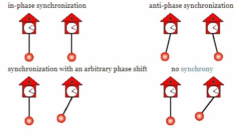
This motion GIF explains/differentiates the terms of synchronize and phase.
(see motion GIF below, readers may need to adjust browser/word-processor settings to view as movie)
The topic is also covered here.
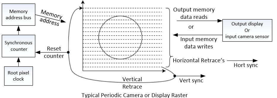
The number-one baseline function of all Graphics Processor Units is to create a video output connector that is itself based on periodic memory-data-reads of a zone of bytes in digital memory, (aka “raster” which is a virtual rectangular graphic zone of pixels that form horizontal lines, and those lines then form a full frame) and then to present that data in a serial stream consisting of the exact periodic/repetitious timed reads of memory (aka Pixel data). The memory-data-reads are then presented as pixel data to a display either as digital or analog pixel data or by adding vertical and horizontal sync pulses to the video output data stream, at the beginning of lines and the beginning of frames.
All Graphics Processor Units (GPU’s) as now named, were previously named “Video-Controller” in the 1980’s up to approximately 1997, where this name change was noted in the industry due to the addition of a super-set of video and graphics functions features.
The basic list consists of:
- Camera-Raster Input
- Block-Line-Transfer (BLITTER) hardware (HW) accelerators
- Texture-Fill (aka Polygon-Fill HW accelerators)
- RGB to YUV and YUV to RGB real-time Color-Conversion HW accelerators
- Motion-Compensation HW accelerator for movie video playback (de-compression)
What about the synchronizing and or phase locking of multiple displays and/or camera inputs? Especially to the pixel sync/lock level? It is still largely ignored (as of July 2021), rather than worked in as one of the basic core GPU functions by the key GPU suppliers.
The following paragraphs will detail multiple design concepts, benefits and issues of designing with GPU’s
4. Multi-Display Human-Eye-Brain Visual Data Processing Issues:
There are three issues that impact human interaction with single and multi-displays regarding display timing.
First: image tearing, for both single and multi-display systems.
Second: eye strain due to out of phase, and even out of sync, multiple nearby displays. Tearing and eye strain impact is heightened when motion such as in animations are split across multiple displays. “Video walls” are engineered specially to get this right, and are phase locked on all displays of such systems.
Third: ability of the human brain to process constantly changing visual data, both in intensive situations (such as a fighter plane pilot), and for long multi-hour periods from multiple displays.
The first and second issues are so closely intertwined with frame rates and multi-head frame sync/phase-lock, that it is often better to discuss them together as one issue. They are usually fixed or fail as one larger issue.
Without synchronization, and better yet, phase-locking of the vertical-sync refresh, users will often see image “tearing” artifacts as the displays are updated. This can happen even in single display configurations. Default settings tempt users and end-product designers to use the super-fast AMD and Nvidia graphics x86 cards to transmit at maximum rate, up to 250 Hz frame-rate, and also to internally update the GPU’s memory display data buffer at up to 250 Hz. When a monitor can only perform at 60Hz refresh rate, the user will experience visual “tearing” as a full frame of new data does not get to the display, before the next frame update-data is being sent to the display. Video driver software (such as Nvidia’s V-Sync) is supposed to prevent this by limiting the GPU’s internal final video buffer (just before transmission) update, transmission (on the cable to the display) frame rate, to match the display’s frame-rate limits.
Thus the most common visual tearing issue is when the GPU chip and card design implementation re-draws its own frame buffer before it can complete the transmission to the display. Or said another way, the GPU “double buffering” is out of phase-lock with the video frame transmission’s.
Are high frame rates for displays needed on desktops or on automobile instrument panels? In general, no. Even Hollywood widescreen movies rarely run at excessive frame rates, and digital versions are rarely over 60 frames per second.
5. Genlock (video frame, line, or pixel timing synchronization to an external source):
Genlocking, a video electronics industry term for over 50 years, can vary including 1-slave-horizontal-line at a time being re-locked to another video master source line-sync, closely enough such that transparency color-key overlay feature can be affected. The slave raster video pixel clock can drift from a close enough match, within about 2 lines of video. This is enough to usually work achieving a frame of Genlocking, 1 line at a time. Genlocking is very sensitive to any noise flaws in the master video source. Common signal imperfections of noise will cause a loss of slave pixel clock sync and thus slave line sync, with resultant large screen jerks, and then sync/lock recovery.
Genlocking Variations of Implementation:
- Frame-sync is the most modest form of video sync (aka genlock)
- Line-sync implies both Frame and Line sync
- Pixel sync, implies all three- Frame, Line, and Pixel sync, being the most capable of delivering synchronized video oriented functions.
These variations of genlock range from milli-second to pico-second accuracy, and different levels of functional robustness (ability to hold sync or recover from sync loss).
Genlocking is also somewhat historically expensive to implement done by creating pixel clocks, not with classic common low cost PLL’s but more commonly made with a dedicated non-multiplied or divided single frequency crystal oscillator for slave pixel clock and considerable analog circuits to detect phase errors along with operational circuits and software to react to the pixel clock error-limits management.
Some GPUs have the “slave-to-external-sync” (aka genlock, aka rough/near phase lock) feature to varying degrees of sync or lock accuracy, and of robustness. However, most GPU’s lack this feature. It is fairly easy to integrate this feature, but it is not often implemented as it should be. If properly designed, even multiple brands of GPUs for the same vehicle-dashboard or desktop PC’s and displays, can be phase locked (or often called “genlock-ed”) to an external source such as to another display, an input, or a camera.
In the following paragraphs we will discuss some modern concepts (newer than the early forms of Genlock) that have some similarities to Genlocking. These are Nvidia V-Sync, G-Sync, AMD FreeSync and Mimax V-Lock.
Some video circuit/method IP suppliers (like Mimax Inc of Seattle) frame phase lock (V-Lock) to sub-pixel, display or camera timing. A timing accuracy of 2 nanoseconds in a system of 10 nanosecond pixels is relatively easy to achieve in chips and circuit boards and will be robust in the field over a product’s lifetime.
MiMax V-Lock causes displays to not only be phase locked for removing synchronous display and camera artifacts, camera image splicing and also inter-chip color-key video overlay features to end products.
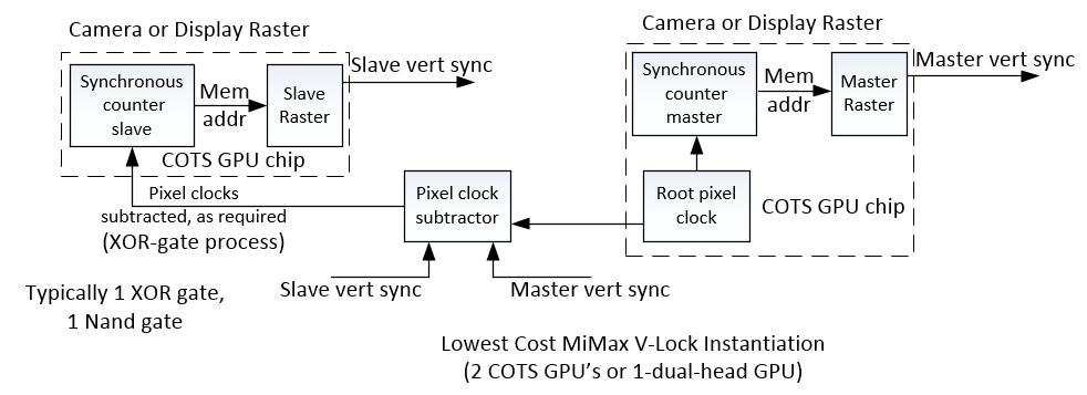
5.1 No-Cost (free) MiMax V-Lock:
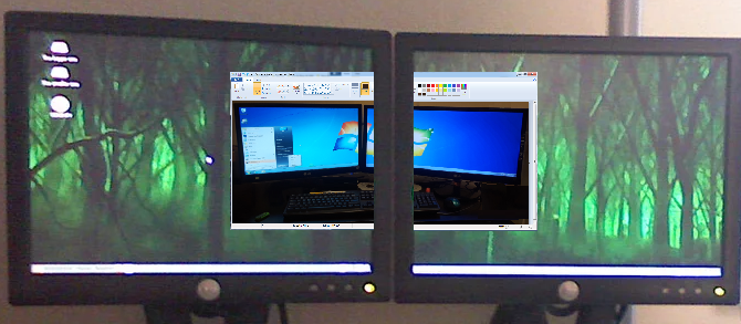
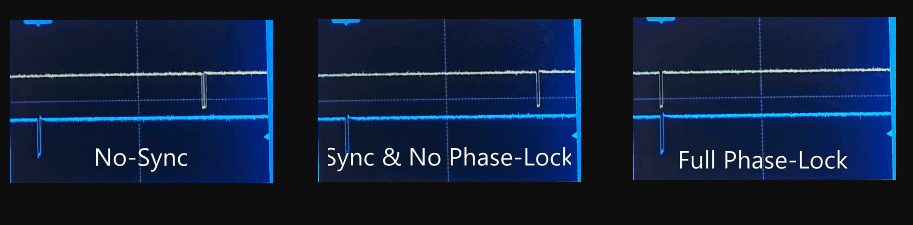
An example of Vertical-Sync is when MiMax V-Lock (a marketing term), is connected to two GPU chips video output, or two raster heads in one Commercial-Off-the-Shelf (COTS) GPU chip video output. Below is a motion GIF and snapshots. Mimax V-Lock uses the same pixel clock for multiple display or camera rasters, thus the one original local cost PLL, serves multiple video raster heads. Clock PLLs are in most all GPUs today, so if there is a failure of the master video source, the slaves will fall back on their internal clock automatically. (see appendix other version of O-scope images)
A dual head video card can drive two desktop displays, turning on/off its V-lock feature.
Below is a graphic of the Mimax V-Lock process that can lock any number of multiple periodic rasters to sub-pixel timing quality level. This is used for improving the viewing experiences and/or reduction of the data sharing process latency. This improves the temporal logical timing association of multiple processes. See “PLV” (phase lock value) further described in the following paragraphs.
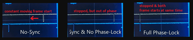
The motion GIF on the previous page shows these three conditions of vertical sync-phase,
to pixel level timing accuracy:
- No-Sync,
- Sync & No Phase –Lock,
- Full Phase-Lock (with auto recovery) modes of operation.
MiMax Video Phase Locking (V-Lock) Technology – See https://mimax.com/
Low cost MIPI-Bus camera image sensors, that lack a sync control input (to act as a slave raster), can also be a master sync source with V-Lock, or a slave sync with V-Lock, if it has a pixel clock-input pin.
Mimax V-Lock permits COTS x86- GPU, Arm-MALI-GPU, or PIC-GPU, or Camera-Image-sensor-chips (Standard-CMOS, DSP-CMOS or CCD) to be fully slave pixel sync to most any external sync or lock signal. V-Lock can hold “lock” theoretically to infinity-time, if there is no cricut failure. Should the phase3 lock of multiple-video-heads (rasters) be lost, due to some severe electrical event, or the user flipping in and out of different video modes, the V-lock re-establishes itself within a few frames automatically (no software is required).
Links:
https://www.tomshardware.com/reviews/nvidia-gsync-monitor-glossary-definition-explained,6008.html
https://boilingsteam.com/amd-freesync-on-a-nvidia-gpu/
https://www.rtings.com/tv/learn/what-is-the-refresh-rate-60hz-vs-120hz
https://www.sunlightinside.com/light-and-health/light-flicker/
MiMax can offer free consulting for V-Lock phase locking implementation into your circuits.
5.2 Nvidia V-Sync , G-Sync, and AMD FreeSync:
Similarly Nvidia offers V-Sync , G-Sync, and AMD offers FreeSync (marketing terms), as methods of reducing tearing in a single display scenario to slow down double buffering of video game data creation, or even for re-building the video playback frames of a compressed DVD MPEG2 movie, by not sending all data to the display monitor, which passes over the temporal display refresh rate pixel paint position. (That is, not to paint new video data to the display, mid-frame timing, and passing over where the current pixel is being painted on the actual display screen, thus avoiding an undesired tearing artifact effect).
Full phase locking – now offered at no cost to the public – is achieved by MiMax V-Lock (method of hardware slave pixel clock subtraction) which works fine at nano-second speeds, combined with or without Nvidia V-Sync, G-Sync or AMD FreeSync functions. V-Lock adds this more accurate and lower cost (free) correction to multiple display timing interactions, and should work fine with Nvidia, AMD, Intel, VIA, Matrox, Silicon Motion, ARM, and PIC family GPU chips or custom FPGA based display rasters.
Even when V-Sync, G-Sync or FreeSync track refresh sync rates, to each of two identical dual-display-screens, if the two displays are not frame phase locked, it is still impossible to present the full dual display new frame video data that crosses the out-of-phase display-screens at the same time.
A choice has to be made in such a scenario, either by living with mid-frame image tearing on one of the displays, or having the two displays update at different phases (of the refresh rate) times, and live with screen to screen image-motion update jerking and display induced eye strain.
Nvidia and AMD methods for GPU to display(s) interactions that produce sync issues, do lessen the two display jerking video data update problem with a software IP semi-fix, that temporarily alters display register values of GPU raster timing controls, and software interrupts to attempt to reduce the out-of-phase condition of two displays to be less out-of-phase. Instead, MiMax locks the two (or more) GPU frame rasters to sub-pixel nano-second timing in a very accurate and fast process, and with no timing change jerks as seen by a person viewing the displays.
The Mimax V-Lock hardware method instantly auto corrects the phase lock of multiple raster display heads should they ever get out of phase lock. The instant/automatic V-Lock auto recovery is not even noticed by a person viewing the displays, but can be seen by an oscilloscope. AMD and Nvidia re-sync and attempts at phase lock, require active software tracking of the vertical sync pulse which lacks accuracy, can vary every time a sync up is attempted, and cannot provide for easy inter-chip color-key overlay, especially when OEM (value-added) video graphics product designs mix the brands and models of GPU chips. V-Lock can work across multiple brands of chips, in a multi-display and multi-camera implementation.
MiMax V-Lock sub-nano second frame and pixel phase lock, also adds on the feature of color-key transparency overlay, where one video can be foreground on-top of the other background. Now drivers can know what gear they’re in!
This inter-chip color-key overlay feature allows for easy methods to place dashboard instruments on top of the back-up camera view, for critical data, such as when a vehicle is in drive or reverse. Most vehicles restrict the back-up camera to only be operational when in reverse. There is no ability to put the shift control position data in an obvious manner on top of the camera view (color-key overlay). This could be made obvious by red-color or green-color outline stripes (works for color and non-color vision drivers) around the camera view to indicate the transmission direction status, which is not always obvious in electric and hybrid cars. Likewise, side camera views could have danger signals added on top of the camera view, if transparency overlay (needing V-Lock) is used.Mimax offers limited no cost phone/email/video-conference help to firms of all sizes to add no cost V-Lock to products.
5.3 New DPS Type Camera Image Sensor:
This Digital Pixel Sensor (DPS), is a new type of CMOS camera sensor with one very critically good feature. Rather than the standard CMOS camera method of off-loading image data via a “running shutter” that grabs about 5% of the image, then the next 5%, then next 5%. the DPS has a full frame instant shutter, like the expensive classic CCD camera sensors.
Classic CMOS running-shutters have serious image tearing issues, when the viewing scene is of things like moving cars. CCD camera sensors and supporting circuits are expensive and consume multiples of wattage that CMOS sensors do. The DPS offers the best of both scenarios of CMOS and CCD sensors. The DPS silicon-dies typically have fewer pixels, as it needs more silicon space for internal copper via’s. However that is not a serious DPS drawback. For ADS systems, 5 million pixel CMOS sensors are a waste of large pixel counts and massive pixel data volumes cannot be consumed in real-time. The camera designs command the camera to typically combine pixels of 4×4 or even 16×16.
DPS-CMOS image sensors, now with full frame shutter, create the desire for OEM multi-camera, or ADS, product designers to phase lock (V-Lock) the camera sensor to the processing of camera data and to the displays. Full frame lock at pixel timing quality levels achieves the maximum rate that data can be processed not just by the human eye, but also by a vehicle’s ADS (auto driving system).
https://image-sensors-world.blogspot.com/2018/02/sony-presents-gs-sensor-with-adc-per.html
February 13, 2018 Sony Presents GS Sensor with ADC per Pixel
https://isl.stanford.edu/~abbas/group/papers_and_pub/isscc_94.pdf
A CMOS Area Image Sensor with Pixel Level A/D Conversion
https://isl.stanford.edu/groups/elgamal/abbas_publications/C093.pdf
Digital Pixel Image Sensors. The DPS architecture employs an ADC per pixel
5.4 LiDAR versus Cameras:
LIDAR Light-radar, is noted here, as it has been used for Automated Driving Systems (ADS) R&D, and some production cars. However, LiDAR is overly expensive for the car/truck OEM products. As such Tesla Inc is turning to lower-cost multiple cameras in place of LiDAR. Cameras are 2D viewing systems by nature, and can never be as good as LIDAR for distance detection. Thus with other methods like stereo camera views, it’s more critical than ever that the multiple-cameras are fully phase locked, such that the multiple camera video data streams data is exactly temporly locked..
It is additionally better if the multiple cameras are not just frame phase locked, to pixel timing accuracy, as to allow for combining the multiple views to determine distance. But to also transmit in a LossLess zero-latency compression. Mimax Pixel NDC compression is a lossless, instantaneous, compression that uses 2 video heads in the camera or GPU, with low reliance on a processor. MM-NDC It is mostly some added gates and a few more registers of D-flip Flops, several small FIFO’s and a few gates. MiMax Macroblock NCC (compression), requires one additional frame latency.
6. GPU Chip Family Groups for Laptops, Desktops, and Embedded Products:
A strong distinction exists in the market for the x86 bus GPUs that are generally bus peripherals versus the ARM-MALI’s processor GPUs that act as their own hosts (bus masters).
The x86 PCIexpress bus is popular but complex. It is a combination data/address and control bus,
Large, pricier ARM variant processors typically act as bus-hosts to create a PCI express bus (some even have hundreds of external pins, for the PCI express bus). The lowest cost PIC-Processors with basic peripheral GPUs built-in and typically create no host PCIexpress bus, and do still act as hosts, to the video raster portion of the chip via a simpler parallel bus. Like the PIC-processor/GPU chips, most ARM-MALI chips do not bring the PCIexpress bus to the external pins, and also use a simpler internal parallel bus.
Overall, the ARM-MALI-GPU and PIC-GPU better fit the car/truck OEMs and the embedded electronics OEM markets better than the x86 GPU chip families, even though there are exceptions.
6,1 High Power AMD, Nvidia, Intel x86 GPU for Desktop Laptop and Graphic-Card Markets:
Intel is now copying AMD and Nvidia in 2021 to make high-end x86 GPU Peripheral cards again. However most of Intel’s Peripheral (no host) GPU units shipped are built into the motherboard “companion chip” products. The x86-GPU market dominating firms, Nvidia, AMD, and Intel, have convinced much of the public that their 250Hz display refresh is worth 300 watts and $800 dollars, while most video displays are running at 60Hz refresh. Most home and office LCD or OLED displays don’t actually run at these excessive speeds, nor do the physically smaller, more cost sensitive embedded LCD or OLED display products. Most of the transportation industry won’t run these intensely high refresh rates and no product or use requirement is needed for this. The x86 bus implies you will use products for large motherboards on Windows 10, MacOS, or Full Linux (typically Ubuntu, or Redhat/Fedora variant), that have a host bus created by a high end X86 processor and x86 companion chip.
Vehicle Transport industry electronics design engineers with design budgets for cost and wattage almost never use x86 bus GPU chips for the drivers instrument displays, because they must keep product design decisions more focused.
Therefore, despite the fact that General Dynamics Land Systems equipped the US Army Stryker fighting vehicles with a Dell computer/PCI bus/NVidia card, the future of MEMS/HUD systems in vehicles will likely not include x86 chips.
See the appendix for more on the x86 industry.
6.2 Low Wattage ARM-MALI / PIC-GPU (host bus chips), for Embedded Display Markets:
The expense of the artificially large and high wattage x86 chips is the economic push that created many suppliers’ ARM-MALI processor/graphics chip families that have come into such enormous popularity with OEM product makers. The ARM processors are RISC (reduced instruction set processor) mated in a single silicon chip with its embedded graphics chip most often called “MALI”.
ARM RISC (reduced instruction set) processors that trace their beginnings all the way back to the Apple-II, C-64 and Atari-400, have a cost-reducing history to be proud of. ARM names its video controller that always comes in the silicon with the general purpose RISC processor with titles like MALI-600, MALI-900, for video potency levels. PIC is an even further reduced instruction set processor, with quite low end GPUs typically topping out with basic raster function with resolutions like 640×480.
6.3 Market Segment of Low Power GPU-Rasters for Displays and Cameras:
Almost at the opposite end of the market of the x86 high wattage, high cost, ultra-high performance GPU chips are the ARM-MALI(GPU) and the PIC-GPU chips. ARM and PIC are the processors and each has its own GPU. PIC’s have the most budget oriented small GPU’s, though some even have some form of genlock and have pixel lock.
Higher-end MALI GPUs are much more likely to have multiple camera raster input ports, typically in the form a camera MIPI-bus that is common to low cost CMOS camera sensor output-and-control buses. ARM-MALI chips often have ready-to-go free versions of small Linux or even Google-phone-OS.
Microsoft is breaking some ground with a new down-sized Win10 variant that can run on some ARM-MALI chips, which is a large source of legal friction with Intel. Apparently Microsoft Inc. assisted ARM makers to incorporate (or mimic) Intel Inc. specific computational x86 processor circuits, making the Win10 software conversion to the RISC ARM instruction set easier. This ARM-MALI use, and MS-OS make up Microsoft’s lowest cost net-book PC., which is a serious break in transition from costly and high wattage consuming x86 processors.
Higher end MALI’s can cost well over $100 and are commonly found in $800 dollar smartphones. Higher end MALI’s also have hardware accelerator texture fill circuits for video game polygon fill, BLITTER hardware accelerator circuits (block line image transfer), and now also incorporate the ARM-Inc IP of “ARM-FRAME-BUFFER-COMPRESSION” (AFBC).
7. ARM-FRAME-BUFFER-COMPRESSION Local-Display-Macro-Blocks Compression:
AFBC is a method using circuits running in MALI GPUs specifically aimed at reducing power (wattage) consumption in mobile-phones and embedded products with displays. For a user diligently playing a video game, it can be the difference between a 4-hour or 5-hour battery drain out. The AFBC method is named “transaction elimination” by Arm Inc. (Transaction Elimination drawing, copyright Arm Inc).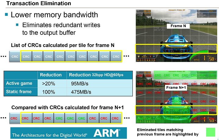
This is a good descriptive name, as “transaction elimination” is the basis of all video compression. That is “to avoid transmitting redundant data”. In the case of AFBC, transmission is just from the MALI GPU to the LCD display, a mere few inches of circuit board distance. A typical year 2021 popular LG phone has a 6.1-inch Quad HD+ display with a screen resolution of 3120 x 1440 pixels, so when 80% of display updates of redundant data can be avoided, that’s a valuable power savings.
8. MiMax, Network-Display-Compression (NDC) of LossLess Pixels and Macro-Blocks:
MiMax has an active patent for lossless pixel NDC (Network Display Compression),which competes directly with Arm Inc’s AFBC patent (already embedded in most ARM-MALI variants). It is aimed instead at any GPU or Camera product, x86 or ARM/PIC embedded that needs to move video data around a vehicle, or over globally. AFBC compression is a macro-block (aka 16×16 pixel macro-cell) only transaction eliminator for extreme local displays to one particular ARM-MALI GPU to display connection(s). MiMax-NDC compression IP runs in both instant pixel or 1-frame-lag macro-block modes, and can also combine frame locking with a mix of video devices. The AFBC function is not instantaneous real-time upon new pixel data occurring, however it is very fast. It is possible to combine Arm-Inc AFBC-IP and MiMax NDC and V-Lock, for the highest degree of high speed, loss-less, video compression (that combination would take some pages of discussion and drawings).
MiMax-NDC is a method that loops back the frame locked raster video data output stream of a GPU for a second loop into a second raster of the GPU (most GPU’s ARM-MALI or x86, have 2 or more rasters , aka 2 or more “heads”). NDC then XOR compares pixels instantaneously in the current real-time pixel data flows, toward the display(s) before pixel or macro-block data is moved in the final video output connection.
Like AFBC from Arm Inc, MM-NDC is in macro-block mode (aka 16×16 pixel macro-cell), and very fast, but not instantaneous. . MM-NDC can also run in real-time (not even 1 frame of latency) instant 1×1 pixel mode, whereas only new pixel data is transmitted to the display . MM-NDC has better temporal correlation between an updated video frame buffer and the macro-block compression process due to all frame buffers (rasters) in the process being temporally frame locked.
9. One GPU Chip, Can Handle 8 Remote Displays:
Another variation of Frame-Locked MM-NDC does the hardware acceleration for compressed video to multiple remote displays showing different subject matter. This may be an overreach for standard vehicles as the designs for those systems should generally avoid high end x86 GPU chips, except in very specific cases such as an auto-driving-system (ADS).
However, this Mimax NDS function is less advantageous for the vehicle industry and better integrated into server farms, where a rack mounted bare-metal computer (software filled with 8 OS-virtual-machines, or 8 OS-containers) is shared by 8 remote users, and the core design benefit is to save on power consumption and equipment costs, by reducing the number of servers and compression cards.
10. 12V Accessories Power Consumption for Vehicles is of Increasing Importance:
Similarly, when a car is parked engine off, but cabin “electrical-accessories–ON” for display’s, radio and other features, the difference of 200 Watts total or 400 watts total means a lot to the battery watt-hour budget, and whether air conditioning will be needed. Automakers and review companies should be quoting the battery (used for starting the engine) current draw, wattage burned, at what ambient temperatures the driver needs to get the air conditioning running, and how long the car can sit in “electrical-accessories–ON” condition. Even in hybrids and full electric cars, usually the 12V battery is used for all electrical accessories.
As more electronics are ramped-up into modern vehicles, this will eventually be picked up by the review publishers and on media outlets like Youtube. It may be hard to measure, but the public is becoming more informed on vehicle reliability issues, cost of maintenance, and features of both pre-purchase new and aging units in the field.
11. Modern LCD/XLED Displays Default to 60Hz:
It’s an oddity that modern LCD/XLED displays default to 60Hz rather than a 30Hz/24Hz or dynamically changing frame rate.
Examples of multi-display systems are ubiquitous in the world today. Typically, most are 60 HZ displays, and some with up to 250 Hz refresh rates are common. Common video cards (graphics cards) and associated software drivers tend to run each display at the highest possible refresh rate that the display is rated for.
Some video gamer magazines make claims that their users can see very high frame rates. There can indeed be some video patterns that high display transmission frame rates improve the final viewing. An example would be, the introduction in the movie Star Wars of the very slow scrolling bright yellow written words, on the high contrast black starry background. Small jumps, in scrolling movement, can be seen, at 24 FPS. It’s an uncommon condition in movies.

Even at 60 Hz, horizontal movement in action such as sports, can show temporal artifacts. Should all displays be run at 120 or 250 FPS because of these semi-rare imagery-motion-contrast scenarios? Even if practical, doubling the frame rate doubles the transmission bandwidth, and that is simply not feasible in most situations.
Systems can be composed from multiple computers with multiple GPUs or one computer sharing a multi-head GPU. Either type can have the displays vertically synchronized or phase locked, but often this function is completely overlooked, and the multiple displays are left to almost random refresh rates and/or refresh out-of-phase conditions.
Even when a user has two identical displays, the dual-output video card (two HDMI ports, or 1 HDMI, 1 analog RGB, or 1 DisplayPort, 1 HSDM port) software driver, at boot-up, or display change set-up, selects the same root pixel clock for both raster scan engines that are in the one “dual-head” GPU chip.
This results in two displays that are in-synchronism, but still out of phase. A typical example is two 60 HZ displays that are randomly 50% (180 degrees of 360 degrees) out of phase. Conceptually similar to looking at an oscilloscope of two 60 Hz sine waves, that are in sync, but out of phase. The reason for “randomness” is that when the video-graphics controller chip, and its host computer are re-booted, or display set-up change occurs, the job of the software video driver writer, is to get the video-graphics-raster head up and running as soon as possible as every millisecond counts for end user satisfaction.
Thus, the first video raster head gets all of its typically 200 control registers set-up, and is running, then the next video raster head gets its registers set-up. Various computer software interrupts of other boot up or applications, are also occurring during video head register set-up. Thus there is no time control over the length of time this GPU chip set up takes. The programmer, as with all applications, video driver, word processor, or game, wants to get the software process done as fast as they can get it done. Thus the real-world time it takes to get video GPU heads set-up done varies every time it happens.
Once set-up, the two video raster display heads, even if running on the same root pixel clock, (because the user has two identical models of displays) typically are about 120 MHz, with the two heads at least in-sync (no rolling bars consciously are visible to the user), but the two displays remain in a constant static out-of-phase condition. Statically the displays are fine, but dynamic image updates, then the viewing issues arise.
However, when the user sends video to the multiple displays, as in a movie or video game across the two displays, then the eye strain problem comes back. AMD and Nvidia tackle this issue by using very high display refresh rates, thus the phase error in absolute time is reduced from a typical 8 msec phase error from display to display at 60Hz refresh rate, to 2 msec at a 250 Hz refresh. From the GPU to the cables and display, almost by straight arithmetic, power consumption rises when the pixel clocks are raised from 120 MHz to 300 MHz, with a doubling of video memory bus widths.
The default setting for almost all CRT displays today is 60Hz. This number comes all the way back from the 1940’s when TV display and signal transmission was in development to be on cathode ray tubes by RCA corp. The 60Hz refresh rate selections by the 1940’s electronics engineers was a very complex and necessary trade-off, for the miracle of TV on 1940’s tube technology, eye-brain motion integration minimum requirements, the amount electromagnetic airwave bandwidth needed, and even included the size of antennas needed.
Later, users in the mid 1990’s began to use CRTs alongside LCD displays. The LCDs can run at much more varied refresh rates than a CRT- both slower and faster. The 60Hz default refresh rate comes directly from the old style television interlace running at 60Hz refresh, and the first video cards needed to support an old CRT and LCD simultaneously at an affordable price. Most of the early LCD displays were designed to take on the job of replacing CRT’s for TV viewing. A single LCD OEM factory could support television and computer display production.
Hollywood 35 and 70mm film wide-screen have used 24 frames per sec at the theater, to view top-of the line movies in widescreen. Even with the introduction of full digital features, the jump to 60 frames is a very good choice for size of files, cost of equipment, and audience satisfaction.
Likewise, video displays on the dashboard of a vehicle also typically update at 60Hz. The annoying close frequency of road lighting can produce slow, annoying beat frequency variations creating user eye strain.
To this day, the world cannot agree on the best display frame rates for all conditions, any more than one vehicle could suit all driving conditions and loads. However, dynamically changing refresh rates may be the winner in the end, where displays are updated at the faster rate when reasonably possible, as data updates are needed.
In summation on compression and frame-rates: The only way to achieve low power, low cost, and high refresh rate combinations, is to send only the changed pixel or macro-block (16 x 16 pixel zones) to the display, or to other video processing stages. Hundreds, if not thousands of patents have been published on video-compression. Most are software, a lesser percentage is hardware. Most of the patents are fine tweaks of existing methods. A few patents are in the range of being called “fundamental patents”, that drill down new usable how-to methods that make large differences in performance, cost and power.
Further reading on modern displays and the automotive industry:
https://www.extremetech.com/extreme/131485-digital-dashboard-why-your-cars-next-instrument-panel-will-be-one-big-lcd
Automotive Cockpit Multi and Dual Display Trend Report, 2020 ($3200.00 USD report PDF):
“Dual Display: Local Chinese Brands and Joint Venture Brands Contend for Model Launches with Dual Display during 2019-2020
This last Reporter Link article says in summary:
Dual display solutions first appeared in 2016….the “one-core multi-screen” solution: the hotspot of multi- and dual- display solutions. The Digital Cockpit 2020 is packed with 4 large displays and 2 small displays:
An Extreme Tech article says “Concept vehicles and soon to be produced vehicles may have high and low LCD displays in the center stack with dual 7- or 8-inch displays. While some higher-end cars have 10-inch displays”.
The future will include LCD instrument panels, two center stack LCDs.
Our commentary: where possible, these displays should be V-locked to a master display and to the cameras.
12. PLV and Why Tesla-Car-OEM is also a Proprietary GPU Chip OEM:
The first reason why Tesla is using a proprietary GPU is surely because displays are becoming core to vehicle products. The highest-end x86 peripheral GPU chips are dangerously in the control of just two companies- Nvidia and AMD. Nvidia and AMD’s GPU chips are pricey and constantly having major architecture changes.
(side note for year-2021 Intel Corp x86-GPU’s: Intel also says they are going to be a major player again in stand-alone GPU chips, and not just to be in the motherboard Intel processor-companion-chip. But this an Intel-Corp promise that is too early to tell the outcome of. It’s fairly clear that Intel intends to at least imitate Nvidia and AMD in the x86-GPU primary markets of high-profit, short-production-run chips for gaming and coin mining OEM end products, that are made with GPUs, rather than industrial OEM end-products. )
Tesla, wants very much to be the OEM technology leader in cars, and potentially even trucks. As such, Tesla needs a GPU chip it can design tune to its needs (at will) , and without fear of chip- end-of-life. This begs the question of, should some group of car/truck OEM’s own and manage their own GPU chip design and fabless production?
The second reason is that there are scientific, commercial/industrial, and press-announcements indications to expect that Tesla’s GPU chips are also being used for Automated Driving Control Systems real-time decision making, (ADS) for steering, throttle, and braking.
It boils down in order of importance: ADS performance, cost, and wattage. ADS is a very difficult, if not a close to impossible concept to become a practical feature. Every technical improvement or cost edge an ADS-OEM can get, they should look into. MiMax is unlikely to be the only electronics or GPU specialist firm that is pursuing GPUs as a solution to real-time tracking of multiple moving risk objects as large-size data-pixels (or macro-blocks) in GPU rasters.
This is because a GPU raster can repeatedly (periodically) read and process more pixel data faster and with perfect periodic timing, and apply Boolean logic on that data. Or better yet, perform these functions from six or more rasters that track different groups of changing data, such as moving objects of other cars, pedestrians, signal lights, dividing lines on roads etc.. If all the rasters are frame locked, then a perfect Phase Locking Value (PLV) can be realized, where the best possible transfer rate of data processing occurs.
The article noted below (see link), discusses PLV in very good detail of how fast a human brain can absorb visual data, and where the synchronizing issues of incoming data are so important. The same is true for multiple computer or graphics processors that funnel processed data from one to the other to the final decision maker.
MiMax Inc has its PLV GPU system filed as an almost 100% done provisional patent document.. As a small IP firm, MiMax is trying to get the message out to the global automobile, truck, and military vehicle manufacturers that there is valuable technology available that can improve display and camera operations and even help ADS integration and reduce latency of final driving decisions.
Phase Locking Value (PLV)
https://journals.plos.org/plosone/article?id=10.1371/journal.pone.0146443
“If two networks can align the oscillatory cycles over time such that the excitability periods are in ‘good’ alignment, then ‘communication’ (information flow) will be optimized.”
13. Summation, Sync Cameras/Displays, Reduction of Artifacts, Power and Bandwidth:
Summation: Phase locking technology can sync multiple rasters/video-buffers and cameras/displays, reducing power consumption, network bandwidth and display artifacts.
Not detailed in this paper are the complex interactions that multiple out-of -sync or out-of-lock displays and cameras can have on a person suffering from various degrees of epilepsy. Studies have been done using V-lock compared to non-phased-locked multiple display systems.
Both ARM Arm-Frame-Buffer-Compression (AFBC) and MiMax Network-Display-Compression (NDC) perform synchronization and compression in differing forms and degrees of compression, at differing speeds of compression, and at differing counts of logic gates needed. MiMax claims to have the lowest gate counts for the most end product benefit,and is usable across almost all GPUs and camera sensor brands and families.
AFBC is in many ARM-MALI chips already, but usable only for display just inches from the MALI-GPU. MiMax-NDC is a more general purpose method for any GPU’s or camera to any video receiver or display be it very close or remote.
V-Sync, G-Sync, Free-Sync of Nvidia/AMD or V-Lock all seek to be solutions for frame synchronization in general “Genlock” terms to differing degrees of accuracy. Frame syncing is for pursuing higher level features that only sync can deliver, or to reduce single screen artifact tearing due to double buffer timing issues or multi-display cross-display jerky motion.
Only MiMax V-lock tackles this at pixel, line and video frame timing levels, and with instant sync recovery. V-Lock can be added to any MALI, x86, or PIC-GPU either internal to the silicon chip, or via external pins of pixel clock-in, and V-sync pulses. V-Lock pixel sync provides sync tight enough in timing (about 200 pico-second accuracy) for color-key-transparency overlay.
The new Digital Pixel Sensors (DPS) are bringing a unique opportunity to combine with Frame and pixel locking, for maximum performance and cost reduction, in Autonomous Driving Systems (ADS) .
There is a high probability that one of the car/truck OEMs will soon bring out a dashboard with identical side-by-side hardware displays.
This dual (or even triple) wide display senario, can be operated in mode-1 of audio-systems and instrument dials, or mode-2 as a very wide “desktop” with a very wide view from a wide-angle-camera covering the vehicle’s rear and rear-sides in totality. This can make for an optional camera view desired by the luxury driver.
This can save 4 seconds of people checking the mirrors on various parts of their vehicles.
Top down view systems are good for parking, but they cannot imitate a good “eyes in the back of your head” view at highway speed. It’s at speed that vehicles need a wide rear camera display, and thus video phase locking across multiple displays. Overall, synching, or better yet full phase locking of rasters/video buffers of cameras and displays reduces visual artifacts and latency of the electronic/computing video processing.
Power and bandwidth reduction (reducing wasteful transmission of redundant video data) is the basis of all video compression. The key to video compression is the latency, circuitry cost, and electrical power. Mimax’s IP uses combinations of raster-buffers of multiple GPU heads. These are novel and easily implemented methods to use COTS GPUs and GPUs with small upgrade modifications such as adding some gates and small pixel/macro-block FIFO’s.
Video compression unfortunately is often overused, by the use of COTS camera modules, that have a built in ARM that uses lossy-compression in each camera around a vehicle perimeter, looking outward. This video data then required decompression. Latency and pixel data accuracy becomes a big victim of this common JPEG/MPEG compression-decompression. The concept of a vehicle automated driving system (ADS) is better suited to non-compressed cameras linked in machine-vision that would use “camera-link” cables from the camera to the ADS computer.
Camera-Link however is very expensive, power consumptive and fragile. A better method would be to still use low cost serial signal cables and compress data using the MiMax-Loss-less NDC method, which uses a dual head GPU rather than an ARM-RISC processor for lossy compression
This white paper was co-authored by:
Mark Chamberlain – Electronics Design Engineer/Programmer
Matt Allard – Technical Marketing of Consumer, Commercial & Industrial Video Systems
Scott McGowan – Electronics Video Systems Design Engineer
Bob Audie Berry – Physicist Consultant Commercial/Military Electronics & Software Systems
Allen MacCannell – Sales of Industrial Computer Systems/Software (allenm@mimax.com)
Appendix
A. More on the x86 GPU chip industry suppliers:
The smaller x86 GPU chip suppliers are X86 GPU from Matrox Inc of Canada, (for more specialized x86 GPUs), Via Inc. of Taiwan (lower end X86 GPU embedded in their motherboard companion chips). A smaller supplier yet, is Silicon Motion Inc, of Taiwan (lower-end stand-alone x86 GPU chip, [yet still with full Windows-OS and Linux-OS desktop software drivers] that can run in x86 peripheral card mode, or run by itself with a small internal general purpose processor, thus also competing to be in the designs of smaller embedded products.)
Where motherboard central processors previously created the bulk of profit in office and home PCs, it is now the high end x86 GPU graphics chips and the associated peripheral cards. The x86 GPU chip market is dominated by its number one selling feature of how many polygons-per-second (aka texture-mapping) it can fill, to make up new frames of moving game objects and backgrounds (most often in the form of video games). The x86 GPU dominating firms, looking to out feature their competitors, have added almost bizarrely high transmission-rates-to-the-displays (via HDMI or DisplayPort) capability.
The average home PC today uses a much more potent video-graphics card than typically is required, and burns much more wattage than the video display process usually needs. Basically, most desktop PC’s today are sort of running video cards that are the equivalent of $100K dollars Cadillac/Mercedes sports-car/land-yachts.
x86 GPU’s usually can handle one camera raster input via a simpler multi-function parallel data bus, or a general purpose LVDS series (but 4 bits wide) data bus. x86 GPU’s are not intended for low power portable equipment as a general theme. x86 GPUs typically do not have a dedicated camera raster input MIPI-bus.
B. MiMax V-Lock O-scope dual display sync-test images:
C. Links of interest
“Tesla Says Its New Self Driving Chip is Finally Baked (2018 Wired article)”
https://www.wired.com/story/tesla-self-driving-car-computer-chip-nvidia/
“2019-Tesla Develops Own Self-Driving AI Chip – Removes NVIDIA”
” CPU, GPU, memory, isp, h.265 video, and nna clusters. Most of these clusters are licensed from IP producers”
https://www.guru3d.com/news-story/tesla-develops-own-self-driving-ai-chip-removes-nvidia.html
“Digital Pixel Image Sensors, The DPS architecture employs an ADC per pixel”
https://isl.stanford.edu/~abbas/group/papers_and_pub/isscc_94.pdf
MIPI low cost CMOS camera bus standard
https://www.mipi.org/specifications/csi-2
“A CMOS Area Image Sensor With Pixel Level A/D Conversion”
https://isl.stanford.edu/groups/elgamal/abbas_publications/C093.pdf
“Overlaying MPC823 Graphics on a Remote Video Source”
https://www.nxp.com/docs/en/application-note/MPC823OVER.pdf
PIC-processor with GPU and LCD output (XGA)
https://www.microchip.com/en-us/product/PIC32MZ1025DAK169
X86 GPU’s shipped
https://www.tomshardware.com/uk/news/gpu-sales-report-q4-2020-jpr
“AMD and Nvidia, the two biggest manufacturers of graphics chips, are getting a new competitor — Intel”
“2021 Nvidia Unveils PCIe version of 80GB A100 Accelerator: Pushing PCIe to 300 Watts”
“Screen tearing means experiencing a technical problem whereby multiple images show in your video display from different frames within one screen draw.”
” option in the video settings. It’s usually called “vertical sync” or “VSync” for short”
“what is Nvidia’s G-Sync technology for preventing screen tearing”
https://www.tomshardware.com/reviews/nvidia-gsync-monitor-glossary-definition-explained,6008.html
“2020 AMD FreeESync on Nvidia GPU?”
“relationship between FPS, V-Sync and Motion Blur”
“Different people will be affected by lights at different flash or flicker rates. Lights that flash or flicker between 16 and 25”
https://www.epilepsy.org.uk/info/photosensitive-epilepsy
“AbilityNet Factsheet – November 2015 Computers and Epilepsy”
“When there is a disconnect between one portion of that feedback loop and another, …. moderate to severe nausea”
https://www.howtogeek.com/241285/why-video-games-make-you-feel-sick-and-what-you-can-do-about-it/
“2020-blog, G sync causing eye strain on Dell 27 Gaming Monitor”
https://forums.blurbusters.com/viewtopic.php?f=2&t=8023
“Phase differences: Video signals generated and output by generator-locked instruments are said to be syntonized”
https://en.wikipedia.org/wiki/Genlock
https://www.rtings.com/tv/learn/what-is-the-refresh-rate-60hz-vs-120hz
Examples where high frame rates improve shown
https://webframes.org/what-is-the-frame-rate-of-human-vision/
“Why 24 frames per second is still the gold standard for film”
FrameLock
https://newsandviews.dataton.com/genlock-framelock-timecode-sync-when-do-i-need-them
“ARM FramE Buffer Compression” (AFBC)
AFBC is a proprietary lossless image compression protocol and format. ………All users of the AFBC modifiers must follow the usage guidelines laid out in this document, to ensure compatibility across different AFBC producers and consumers.”
https://www.arm.com/why-arm/technologies/graphics-technologies/arm-frame-buffer-compression
https://www.kernel.org/doc/html/latest/gpu/afbc.html
Mimax Free V-Lock, low power Video compression (pixel or macro-block), Locked-GPU-ADS (autonomous driving system)
“Automotive Cockpit Multi and Dual Display Trend Report, 2020”
Automotive Cockpit Multi and Dual Display Trend Report, 2020 ($3200.00 USD report PDF):
“Dual Display: Local Chinese Brands and Joint Venture Brands Contend for Model Launches with Dual Display during 2019-2020
D. List of Mimax patents and applications
- US6262695 Method and apparatus for phase-locking a plurality of display devices and multi-level driver for use therewith
- US8139072 Network hardware graphics adapter compression
- US8441493 Network hardware graphics adapter compression
- US10499072 Macros cell display compression multi-head raster GPU
- US Provisional Application No. 63/125,310 Object Macrocells in Frame Locked Rasters for Real-Time Driving, Positive Train Control and General Purpose Anti-Collision Provisional Patent Filed